Chapter 22
VCOs and Phase-Locked Loops
Every converter, processor and radio needs a clock, usually faster than any crystal can provide. A phase-locked loop makes one: it locks a voltage-controlled oscillator to a multiple of a clean reference. This chapter builds a ring oscillator, a phase-frequency detector and a charge pump in both PDKs, derives the linear model that makes the loop stable, and checks it against a transistor-level simulation of the loop locking.
- Explain how a ring oscillator oscillates, and set its frequency with a control voltage in a current-starved VCO.
- Define jitter and phase noise, and relate them to each other and to the power of an oscillator.
- Describe the phase-frequency detector and the charge pump, and their non-idealities: reset pulses, current mismatch and static phase offset.
- Derive the linear model of a charge-pump PLL, and design its loop filter for a given bandwidth and phase margin.
- Simulate a PLL locking in both PDKs and compare its response with the linear model.
Contents
Further learning · RFIC Design with Open-Source Tools
This chapter is where analog design meets radio design. SkillSurf’s companion course, RFIC Design with Open-Source Tools, continues from here in IHP SG13G2: LC oscillators and phase noise, PLL dynamics and phase noise, frequency dividers, fractional-N synthesizers and digital PLLs, and builds the low-noise amplifiers, mixers and power amplifiers of a complete 2.4 GHz transceiver.
22.1 What a phase-locked loop does
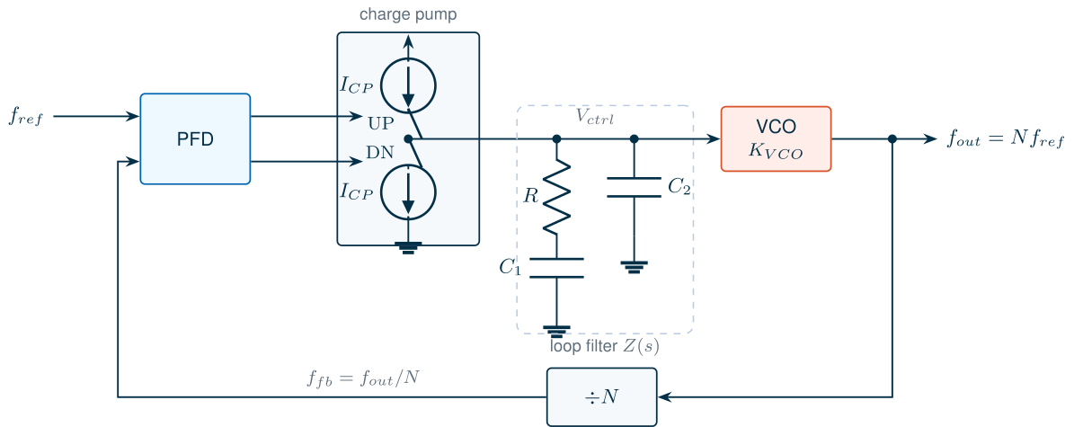
A crystal oscillator gives a frequency accurate to a few parts per million, but only up to some tens of megahertz. A voltage-controlled oscillator (VCO) on the chip reaches gigahertz, but its frequency depends on the process, the supply and the temperature by tens of per cent. A phase-locked loop (PLL) combines the two: it divides the VCO’s frequency by \(N\), compares the phase of the result with the reference, and adjusts the VCO until the two are aligned. In lock the divided output has exactly the reference frequency, so
\[f_{out} = N\,f_{ref}, \tag{22.1}\]with the accuracy of the crystal. Figure 22.1 shows the most common form, the charge-pump PLL [116, 67]: a phase-frequency detector (PFD) compares the reference with the divided output and drives a charge pump, which pushes current pulses into a loop filter; the filter’s voltage \(V_{ctrl}\) tunes the VCO. The PLL of this chapter multiplies a 50 MHz reference by \(N\) = 10 to 500 MHz, the kind of clock that runs the converters of Chapter 21.
22.2 Ring oscillators and the current-starved VCO
A loop of an odd number \(N_s\) of inverters has no stable state: any change at one node travels round the ring and returns inverted. An edge takes one inverter delay \(t_d\) per stage, and the output changes after each trip round the ring, so the period is \(2N_st_d\) and
\[f_{osc} = \frac{1}{2N_s\,t_d}. \tag{22.2}\]In the language of Chapter 11, the ring is a feedback loop whose loop gain has a magnitude of at least one at the frequency where its phase shift is 360°, the Barkhausen condition: each stage contributes 180°/\(N_s\) besides its inversion.
To tune the frequency, the current-starved ring of Figure 22.2 limits the current of each inverter with an NMOS current source \(M_{SN}\), whose gate is \(V_{ctrl}\), and a PMOS current source \(M_{SP}\), biased by a copy of the same current through \(M_{B1}\) and \(M_{B2}\) [55]. Each inverter then charges or discharges its load capacitance \(C_{st}\) with a current \(I\) set by \(V_{ctrl}\), through about half the supply, so \(t_d \approx C_{st}V_{DD}/(2I)\) and
\[f_{osc} \approx \frac{I}{N_s\,C_{st}\,V_{DD}}, \qquad K_{VCO} = \frac{\partial f_{osc}}{\partial V_{ctrl}}. \tag{22.3}\]The VCO gain \(K_{VCO}\), in Hz/V, is what the loop sees. Our VCO has five stages with 1/2 µm inverters (Lmin), 2/4 µm current sources (2Lmin) and 10 fF on each stage, in both PDKs.
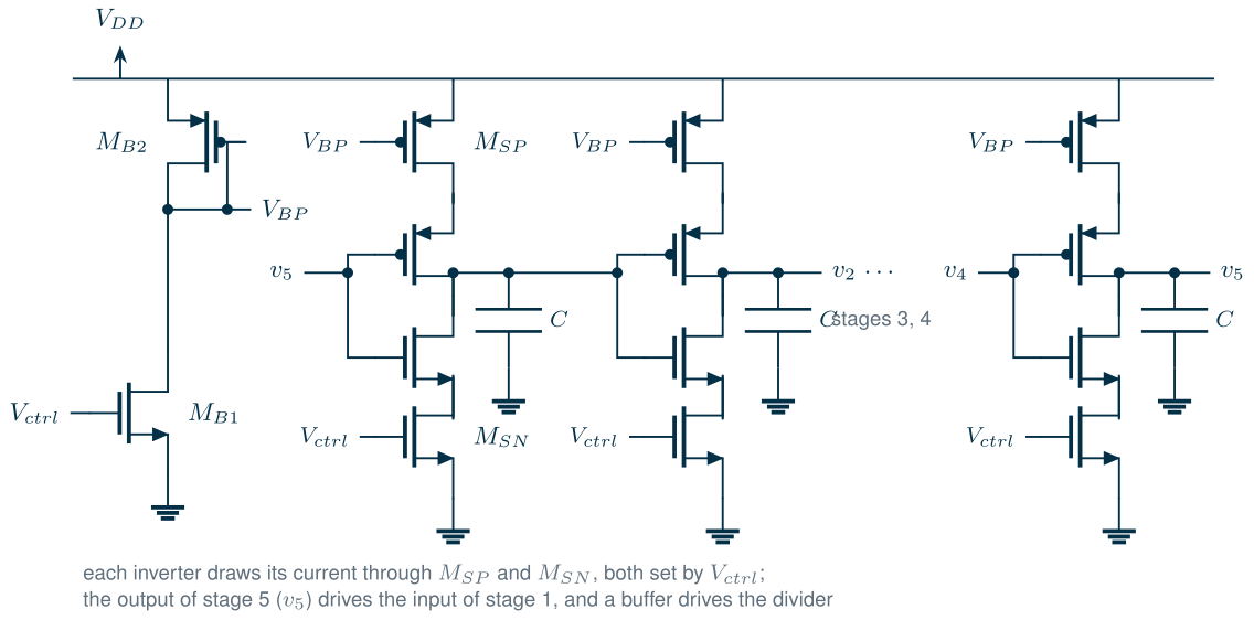
Figure 22.3a shows the simulated tuning curves. The SG13G2 VCO tunes from 32 MHz at \(V_{ctrl}\) = 0.35 V to 896 MHz at 1.2 V, the SKY130 VCO from 67 MHz at 0.75 V to 834 MHz at 1.8 V. Both curves follow the square law of the starving NMOS at low control voltages and saturate at the top, where the inverters’ own transistors, not the current sources, limit the current. At 500 MHz, the frequency of our PLL, \(K_{VCO}\) is 1.97 GHz/V in SG13G2 (at \(V_{ctrl}\) = 0.64 V) and 1.43 GHz/V in SKY130 (at 1.03 V). A large \(K_{VCO}\) covers more of the process spread, but turns every millivolt of noise or ripple on \(V_{ctrl}\) into more frequency error.
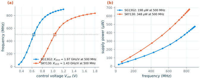
The power rises roughly in proportion to the frequency (Figure 22.3b): each cycle charges and discharges every stage once, and the bias branch draws a copy of the stage current. At 500 MHz the VCO draws 198 µW in SG13G2 and 348 µW in SKY130, 395 and 696 fJ per cycle; SKY130 pays 1.8 times more per cycle, mostly for its 1.5 times larger supply.
22.3 Jitter and phase noise
The noise of the transistors makes the edges of an oscillator arrive early or late. In the time domain this is jitter: the period jitter \(\sigma_T\) is the standard deviation of one period. In a free-running oscillator the timing errors of successive periods add up: the error of an edge relative to an ideal clock is a random walk, whose variance grows in proportion to time, \(c\,t\) [121, 119]. In the frequency domain the same noise spreads the oscillator’s spectrum around \(f_0\), and the phase noise \(\mathcal{L}(\Delta f)\) is the power in 1 Hz at an offset \(\Delta f\) from the carrier, relative to the carrier, in dBc/Hz. For white noise sources the two are related by [121]
\[\mathcal{L}(\Delta f) \approx \frac{f_0^2\,c}{\Delta f^2} = \frac{f_0^3\,\sigma_T^2}{\Delta f^2}, \qquad \sigma_T = \sqrt{c/f_0}, \tag{22.4}\]a spectrum falling at 20 dB per decade. (Close to the carrier, flicker noise makes it fall faster, and very close it flattens; Eq. (22.4) holds in between.)
What sets \(c\)? Each edge of a ring oscillator is the charging of a capacitance by a transistor current, and the thermal noise of that current, integrated over the edge, moves the time at which the node crosses its threshold. Hajimiri, Limotyrakis and Lee [120] and Abidi [122] showed that, for a ring of inverters, the result depends to first order on \(kT/P\) and on the supply and threshold voltages, but not on the number of stages: at a given frequency, halving the phase noise power costs twice the oscillator power. This is why oscillators are compared with a figure of merit that removes frequency, offset and power,
\[\mathrm{FoM} = -\mathcal{L}(\Delta f) + 20\log_{10}\frac{f_0}{\Delta f} - 10\log_{10}\frac{P}{1\ \mathrm{mW}}, \tag{22.5}\]and why LC oscillators, whose resonator filters the noise ([115]), reach lower phase noise than rings for the same power. ngspice cannot simulate the transistor noise in a transient simulation (Chapter 20), so this chapter does not quote a simulated jitter; the references give hand formulas for it. Inside a PLL the loop corrects the VCO’s slow phase wander: at offsets well below the loop bandwidth the output follows the reference’s phase noise (multiplied by \(N\)), and above it the VCO’s own. A wider loop bandwidth therefore suppresses more of the VCO noise, as long as the reference is clean.
22.4 The phase-frequency detector and the charge pump
The phase-frequency detector of Figure 22.1 is two D flip-flops with their inputs tied to 1, clocked by the reference and by the divided output, and reset together by an AND gate [116, 117]. If the reference edge comes first, UP goes high and stays high until the feedback edge arrives; then both flip-flops are briefly high, and the AND gate resets them. DN works the same way when the feedback leads. The width of the UP or DN pulse is the time between the two edges, so the PFD measures phase. If the frequencies differ, the faster input produces pulses on every edge while the other rarely does, so the PFD also drives the loop in the right direction to pull in the frequency, which a simple phase detector cannot.
The charge pump turns the pulses into charge: a PMOS current source \(I_{CP}\) switched on by UP, and an NMOS current source \(I_{CP}\) switched on by DN. For a phase error \(\Delta\phi\) between the reference and the divided output, the average output current over a reference period is
\[\overline{I_{CP}} = I_{CP}\,\frac{\Delta\phi}{2\pi}, \tag{22.6}\]linear between −2π and 2π. Our charge pump uses 20 µA, mirrored from an ideal reference current through 2/4Lmin NMOS and 6/4Lmin PMOS sources, with minimum-length switches. The flip-flops and the AND gate are behavioural (ngspice’s XSPICE digital models, with 20 ps flip-flop delays and a 100 ps AND gate), so that the reset pulse is about 0.15 ns long. Figure 22.4 shows the average current into a fixed voltage at the lock point of each VCO. It follows Eq. (22.6) over the full ±2π, within a few per cent. The UP and DN currents are not exactly 20 µA, nor equal: 21.3 and 20.2 µA in SG13G2, 19.1 and 19.9 µA in SKY130, because the output voltage gives each current source a drain-source voltage different from that of its diode-connected reference, and the finite output resistance of Chapter 8 does the rest.
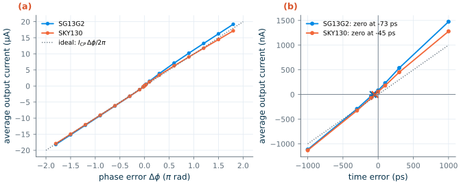
Close to zero phase error the characteristic is not ideal (Figure 22.4b). Both currents flow during every reset pulse, and the switches inject charge when they turn on and off, so the charge pump delivers 83 nA (SG13G2) and 58 nA (SKY130) even at zero phase error. The loop settles where the average current is zero: with the feedback edge 73 ps (SG13G2) and 45 ps (SKY130) ahead of the reference, a static phase offset. Matched UP and DN currents (for example with a replica amplifier that copies the output voltage onto the reference branch) and short reset pulses reduce it [67]. The reset pulse must not be too short, though: if the pulses were shorter than the time the current sources need to turn on, small phase errors would produce no current at all, a dead zone in which the loop does not respond.
22.5 The linear model of the loop
Once the loop is close to lock, it behaves like a linear system in the phase domain [116]. Each block has a transfer function: the PFD and charge pump turn phase into current with \(I_{CP}/2\pi\) (Eq. 22.6), the loop filter turns current into voltage with its impedance \(Z(s)\), the VCO integrates frequency into phase, \(2\pi K_{VCO}/s\), and the divider divides the phase by \(N\). Around the loop:
Key equation · Loop gain of a charge-pump PLL
\[G(s) = \frac{I_{CP}}{2\pi}\,Z(s)\,\frac{2\pi K_{VCO}}{s}\,\frac{1}{N}, \qquad Z(s) = \frac{1 + sRC_1}{s\,(C_1 + C_2)\,\left(1 + sRC_s\right)}, \quad C_s = \frac{C_1C_2}{C_1 + C_2}. \tag{22.7}\]The output phase follows \(N\) times the reference phase with the closed-loop response \(N\,G/(1+G)\).
The loop has two integrators: the VCO, and the capacitor \(C_1\) that stores the charge. Two integrators alone give a phase of −180° at all frequencies, and the loop would oscillate. The resistor \(R\) adds a zero at \(\omega_z = 1/(RC_1)\) that lifts the phase back; \(C_2\), much smaller than \(C_1\), adds a pole at about \(\omega_p = 1/(RC_2)\) that smooths the voltage steps the current pulses make on \(R\). Between the zero and the pole \(\vert Z\vert \approx R\), and the loop gain crosses unity at
\[\omega_u \approx \frac{I_{CP}\,R\,K_{VCO}}{N}. \tag{22.8}\]Placing the zero a factor \(b\) below \(\omega_u\) and the pole a factor \(b\) above gives a phase margin (Chapter 11) of
\[\mathrm{PM} \approx \arctan b - \arctan\frac{1}{b}, \tag{22.9}\]62° for \(b\) = 4. The loop is a sampled system, since the PFD compares phases only once per reference period, and the continuous-time model is accurate only if \(f_u\) is well below the reference frequency. Gardner’s sampled analysis shows the loop becoming unstable as the bandwidth approaches a sizeable fraction of \(f_{ref}\) [116], so designs keep \(f_u\) about a tenth of \(f_{ref}\) or less.
Worked example 22.1 · Designing the loop filter
Take \(f_u = f_{ref}/20\) = 2.5 MHz, \(b\) = 4, \(I_{CP}\) = 20 µA and \(N\) = 10. From Eq. (22.8), \(R = N\omega_u/(I_{CP}K_{VCO})\); then \(C_1 = b/(\omega_uR)\) and \(C_2 = 1/(b\,\omega_uR)\).
SG13G2 SKY130 \(K_{VCO}\) at 500 MHz 1.97 GHz/V 1.43 GHz/V R 3.99 kΩ 5.49 kΩ C1 63.8 pF 46.4 pF C2 3.99 pF 2.90 pF The same bandwidth needs a smaller R in SG13G2, whose VCO gain is larger. \(C_1\) is large: 63.8 pF of MIM capacitance is 42 500 µm² in SG13G2, a square of about 0.2 mm on a side. A smaller \(I_{CP}\) would allow a proportionally larger R and smaller capacitors, at the price of more noise from R and from the charge pump.
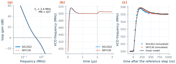
Figure 22.5a plots \(\vert G\vert\) for both designs: they cross unity at 2.4 MHz with a phase margin of 63°; the approximation of Eq. (22.8) aimed at 2.5 MHz, and Eq. (22.9) at 62°. The two curves coincide, since each filter compensates its own \(K_{VCO}\).
22.6 Locking
We simulated the complete PLL: the VCO and the charge pump at transistor level in each PDK, the PFD and a divide-by-10 counter as behavioural XSPICE models, and the loop filter of Worked example 22.1. The control voltage starts where the VCO runs at 400 MHz, 20 % below its target. At 2 µs, once the loop has locked, the reference frequency steps by +1 %, from 50 to 50.5 MHz.
Figure 22.5b shows the VCO frequency, averaged over each reference period. At first the VCO is 100 MHz too slow, so the feedback edges fall further behind the reference in every period, and the PFD answers with ever longer UP pulses. The frequency reaches 500 MHz within about 0.1 µs, overshoots to 516 MHz, and settles: it stays within 0.2 % of 500 MHz after 0.71 µs in SG13G2 and 0.73 µs in SKY130. After the reference step, the loop follows to 505 MHz (Figure 22.5c). Its response matches the linear model of Eq. (22.7): an overshoot of 17.4 % (SG13G2) and 17.9 % (SKY130) of the step, against 17.4 % predicted, and settling to within 2 % of the step in about 0.7 µs, less than two periods of \(f_u\).
In lock, the charge pump’s pulses leave a small ripple on \(V_{ctrl}\), 1.0 mV peak to peak in SG13G2 and 1.5 mV in SKY130, repeating at the reference frequency. Through \(K_{VCO}\) it modulates the VCO frequency periodically and appears in the output spectrum as reference spurs at \(f_{out} \pm f_{ref}\). A larger \(C_2\), a smaller static phase offset (shorter overlap of UP and DN), or a lower \(K_{VCO}\) reduce them; the loop bandwidth must then be chosen again.
Table 22.1. The PLL of this chapter in both PDKs (simulated, tt, 27 °C; fref = 50 MHz, N = 10, ICP = 20 µA).
| SG13G2 | SKY130 | |
|---|---|---|
| VCO tuning range | 32–896 MHz | 67–834 MHz |
| KVCO, Vctrl at 500 MHz | 1.97 GHz/V, 0.64 V | 1.43 GHz/V, 1.03 V |
| VCO power at 500 MHz | 198 µW | 348 µW |
| Charge pump UP / DN current | 21.3 / 20.2 µA | 19.1 / 19.9 µA |
| Static phase offset (feedback early) | 73 ps | 45 ps |
| Loop bandwidth fu, phase margin | 2.4 MHz, 63° | 2.4 MHz, 63° |
| Lock time from 400 MHz (to 0.2 %) | 0.71 µs | 0.73 µs |
| Overshoot after a +1 % reference step (linear model: 17.4 %) | 17.4 % | 17.9 % |
| Ripple on Vctrl in lock | 1.0 mV | 1.5 mV |
Try it · The PLL script
Every number in this chapter comes from
tools/figs/ch23_pll.py:python3 tools/figs/ch23_pll.py vco pfd lock. Three experiments: (1) setBSEPto 2 and rerunlock --resim: by Eq. (22.9) the phase margin falls to 37°; how large is the overshoot now? (2) SetFCto 10 MHz, a fifth of the reference frequency: does the loop still follow the linear model? (3) Change the AND gate’s delay inxspice_modelsfrom 100 ps to 20 ps and rerunpfd: what happens to the static phase offset, and to the characteristic near zero?
- A ring of Ns inverters oscillates at 1/(2Nstd); starving its inverters of current makes a VCO. Ours tunes over more than a decade, with KVCO = 1.97 (SG13G2) and 1.43 GHz/V (SKY130) at 500 MHz, for about 400 and 700 fJ per cycle.
- Jitter and phase noise are two views of the same random timing error; for white noise, 𝓛(Δf) ≈ f03σT2/Δf2, and a ring oscillator’s noise falls only with its power.
- The PFD and charge pump deliver an average current ICPΔφ/2π over ±2π, and also detect frequency; reset pulses, current mismatch and charge injection leave a static phase offset of tens of picoseconds.
- The loop gain of a charge-pump PLL has two integrators; a resistor in series with the loop capacitor adds the zero that makes it stable, and Eqs. (22.8)–(22.9) design it for a bandwidth and a phase margin.
- The simulated PLLs lock from 400 MHz in about 0.7 µs in both PDKs, and follow a reference step with the 17 % overshoot that the linear model predicts.
Further reading
- SkillSurf, RFIC Design with Open-Source Tools: the next course. Its Part IV picks up from this chapter with LC VCOs, phase-noise budgets, dividers, fractional-N and digital PLLs, and its other parts design the rest of a radio.
- B. Razavi, Design of CMOS Phase-Locked Loops [67]: from oscillators and phase detectors to the analysis and design of complete PLLs, at the level of this course.
- F. M. Gardner, “Charge-pump phase-lock loops” [116]: the linear model of this chapter, and its stability limit; I. A. Young, J. K. Greason and K. L. Wong [117] for an early, complete CMOS clock-generator PLL; J. G. Maneatis [118] for self-biased loops whose bandwidth tracks the reference.
- A. Hajimiri, S. Limotyrakis and T. H. Lee [120] and A. A. Abidi [122]: how to estimate the jitter and phase noise of ring oscillators by hand; A. Demir, A. Mehrotra and J. Roychowdhury [121] for the theory linking the two.