Chapter 16
Physical Verification and Post-Layout Simulation
A layout is only finished when it passes design-rule and layout-versus-schematic checks and still meets its specification with the extracted parasitics in place. This chapter takes the course OTA of Chapter 15 through all three in both PDKs, with the tools of IIC-OSIC-TOOLS.
- Run the DRC decks of SG13G2 (KLayout) and SKY130 (KLayout and Magic), read their reports and judge a reported violation.
- Run LVS with KLayout and with Magic and Netgen, write a reference netlist that describes what is drawn, and debug a mismatch.
- Extract the parasitic capacitances of a layout with Magic and simulate the extracted netlist in the testbench of the schematic.
- Check what the block still needs before tape-out: antenna rules, density and fill.
Contents
16.1 The three checks
Figure 16.1 shows the flow. Design-rule checking (DRC) compares the geometry with the foundry’s rules and needs only the layout. Layout versus schematic (LVS) extracts the devices and their connections from the layout and compares them with a reference netlist. Parasitic extraction (PEX) writes a netlist of the layout with the resistance and capacitance of its wires, which then replaces the schematic in the testbenches of Chapter 12. A failure at any stage sends you back to the layout of Chapter 15.
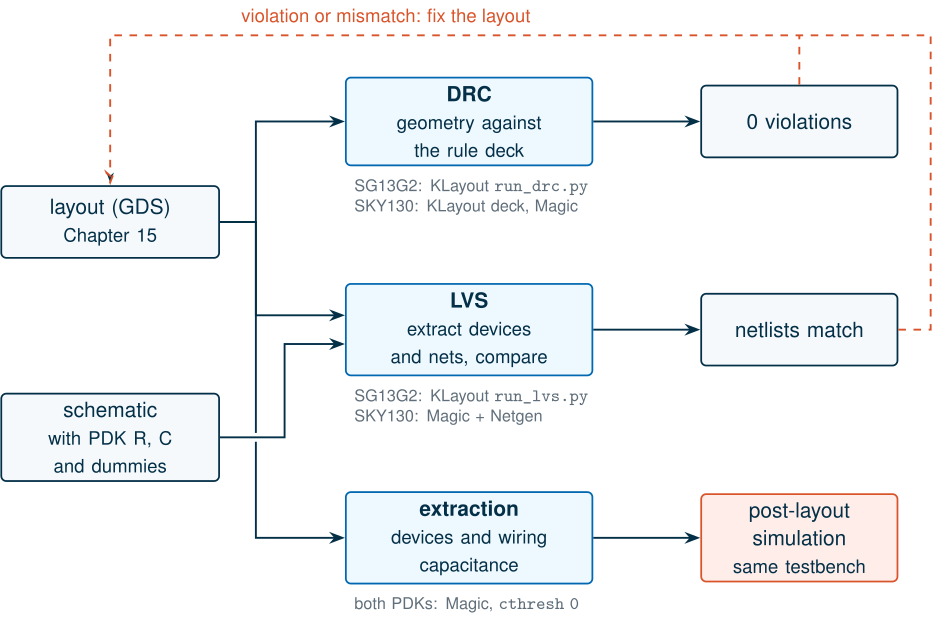
tools/layout/verify.py runs all of it for the course OTA.All three run in batch mode in IIC-OSIC-TOOLS. For the course OTA one command does everything and writes a summary for each PDK to tools/layout/<pdk>/verify.json:
cd /foss/designs/art_of_aicd
python3 tools/layout/ota_layout.py sg13g2 sky130   # the layouts of Chapter 15
python3 tools/layout/verify.py                     # DRC, antenna, LVS and extraction, both PDKs
The sections below show what the script runs, so that you can do the same for your own block.
16.2 Design-rule checking
A DRC deck is a program: it derives layers from the drawn ones (gate = poly and active, for example), measures widths, spacings and enclosures, and reports every shape that breaks a rule. Each PDK ships its own decks [14, 20]:
# IHP's KLayout deck: all rule tables except density (a chip-level check), split over 4 processes
python3 $PDK_ROOT/ihp-sg13g2/libs.tech/klayout/tech/drc/run_drc.py \
    --path=ota2s.gds --topcell=ota2s --run_dir=drc --mp=4 --no_density
# the antenna rules are a separate run (Chapter 17)
python3 $PDK_ROOT/ihp-sg13g2/libs.tech/klayout/tech/drc/run_drc.py \
    --path=ota2s.gds --topcell=ota2s --run_dir=antenna --antenna_only
klayout ota2s.gds -m drc/ota2s_ota2s_full.lyrdb       # browse the markers on the layout
# the KLayout deck (front end and back end of line)
klayout -b -r $PDK_ROOT/sky130A/libs.tech/klayout/drc/sky130A_mr.drc \
    -rd input=ota2s.gds -rd top_cell=ota2s -rd report=drc.lyrdb \
    -rd feol=true -rd beol=true -rd floating_met=false -rd offgrid=true -rd seal=false
# Magic's full rule set, from a Tcl script run with  magic -dnull -noconsole -rcfile .../sky130A.magicrc
#   gds read ota2s.gds; load ota2s; drc style drc(full); drc check; drc catchup
#   puts [drc list count total]; puts [drc listall why]
The course OTA passes: zero violations in the full SG13G2 deck and in its antenna rules, and zero in the SKY130 KLayout deck (Table 16.1). Getting there took one fix, and it is a typical one. The first SKY130 run of Magic’s full rule set reported one violation, rpm.1: width of RPM < 1.27 µm, on the nulling resistor: the generator had drawn the resistor’s implant layer (rpm, which marks the p+ poly resistor) only 1.09 µm wide. The layout script now widens it to 1.40 µm. Magic still reports the rule at the edge of the resistor, and the cell that its own generator produces, with or without a guard ring, fails the same rule on its own, while the KLayout deck passes the same GDS. That is a disagreement between tools on a PDK cell, not an error in the block. The right response is to understand it, check it with the second deck, and record it, as a foundry would ask you to do for a waiver. In SKY130, always run both decks: the KLayout deck checks widths, spacings, implants and the contact and metal layers but not the device rules poly.7, poly.8, licon.5 and licon.11, which Magic’s full rule set enforces; Chapter 23 shows a transistor that passes the one and fails the other.
Table 16.1. Verification of the course OTA (IIC-OSIC-TOOLS 2026.10).
| Check | SG13G2 | SKY130 |
|---|---|---|
| DRC, KLayout deck | 0 violations (all tables except density) | 0 violations (FEOL and BEOL) |
| DRC, second check | antenna rules: 0 violations | Magic drc(full): 1, rpm.1 on the PDK resistor cell |
| LVS | KLayout (run_lvs.py): netlists match |
Magic + Netgen: circuits match uniquely |
| Extracted devices (fingers, before combining) | 92 | 50 |
| Wiring capacitors, total | 36, 169 fF | 33, 144 fF |
Reading violations. Every violation has a rule name, a short description and a marker on the layout; the rule names lead you to the layout-rules document [16, 18]. Fix them in the generator or script that drew the shape, not in the GDS: the next regeneration would bring the error back. The violations that appear most often in analog blocks are spacings between wells of different potential, enclosures of contacts and vias at the end of a wire, minimum areas of small metal islands left over at via stacks, and the device-specific rules of resistors and capacitors.
16.3 Layout versus schematic
LVS answers a simple question: is the drawn circuit the circuit you simulated? It works in two steps. Extraction recognizes devices from layer combinations (a gate where poly crosses active inside an implant, a resistor where the resistor marker covers poly, a capacitor where the MIM layer overlaps its plates), measures their parameters and follows the conductors from shape to shape through contacts and vias to build the netlist. Comparison matches that netlist with the reference: devices by type and parameters, nets by their connections, and finally the named pins.
python3 $PDK_ROOT/ihp-sg13g2/libs.tech/klayout/tech/lvs/run_lvs.py \
    --layout=ota2s.gds --netlist=ota2s_lvs.spice --topcell=ota2s --run_dir=lvs \
    --combine_devices --disable_tap_extraction
klayout ota2s.gds -m lvs/ota2s.lvsdb       # the netlist browser shows every device and net, matched or not
# Magic extracts, Netgen compares (the PDK's setup file tells Netgen how to treat each device)
#   magic script:  gds read ota2s.gds; load ota2s; extract all; ext2spice lvs; ext2spice -o ota2s_ext.spice
netgen -batch lvs "ota2s_ext.spice ota2s" "ota2s_lvs.spice ota2s" \
    $PDK_ROOT/sky130A/libs.tech/netgen/sky130A_setup.tcl lvs.out
Two things make LVS pass where a naive attempt fails.
The reference must describe what is drawn. The schematic of Chapter 12 has an ideal \(C_c\) and \(R_z\) and no dummies. The reference netlist of the layout, ota2s_lvs.spice, is written from it by tools/layout/lvs_netlists.py: \(R_z\) and \(C_c\) become the PDK’s poly resistor and MIM capacitor with their drawn dimensions, and the dummy transistors of each row are added with all their terminals on the rail. The layout has 92 (SG13G2) or 50 (SKY130) separate fingers; both tools combine parallel fingers of the same size into one device before comparing, so the reference may list \(M_7\) as one transistor of 24 fingers.
The reference must be in the form the tool reads. IHP’s KLayout deck expects CDL-style element lines: M for transistors, R and C with the model name, as Xschem writes them in LVS mode (each SG13G2 symbol has an lvs_format for this). A netlist in simulation form, with every device as a subcircuit call (XM1 ...), is read as an empty schematic: the run reports that the netlists do not match, and nothing more. Our first SG13G2 run failed exactly like that. Netgen, on the other hand, reads the simulation form of SKY130 directly.
Common pitfall · An LVS mismatch with no details
When LVS reports a mismatch but lists no unmatched devices or nets, suspect the reference before the layout: a netlist the reader did not understand, a top cell with another name, or ports in different case. Open the LVS database in KLayout’s netlist browser, or load it in Python (
klayout.db.LayoutVsSchematic) and list the circuits it read from each side. In our failed run the schematic side held no circuit at all. A mismatch in the layout itself, by contrast, comes with names: an unmatched net (a missing via, two nets shorted by an overlapping shape), an unmatched device (a dummy that is not in the reference, a finger with the wrong length) or a pin label on the wrong layer.
The --disable_tap_extraction option in the SG13G2 command tells the deck not to extract the substrate and well taps as devices of their own, so that the reference, like a Magic and Netgen comparison, does not have to list them.
16.4 Parasitic extraction
Magic extracts the same devices as for LVS and, with a capacitance threshold of zero, every capacitance of the wiring: area and fringe capacitance of each net to the substrate and coupling capacitance between nets that overlap or run side by side [40]. The same script works in both PDKs, with each PDK’s Magic setup: Check the extracted netlist around capacitors: for a SKY130 MIM capacitor, Magic’s full extraction adds a capacitance directly between the two plates, on top of the device itself, about 4 % of the capacitor’s value (Chapter 26).
# magic -dnull -noconsole -rcfile $PDK_ROOT/<pdk>/libs.tech/magic/<pdk>.magicrc pex.tcl
gds read ota2s.gds
load ota2s
extract do local
extract all
ext2spice lvs
ext2spice cthresh 0
ext2spice format ngspice
ext2spice -o ota2s_pex.spice
The extracted SG13G2 OTA has 36 capacitors adding up to 169 fF; the SKY130 one has 33 adding up to 144 fF. The largest ones tell you which nodes matter: in SG13G2, 70 fF from the tail node to ground (long routes from the input pair to the tail transistors), 35 fF on the output and 11 fF from the first-stage output \(x_1\) to the supply; in SKY130, 43 fF between the two plates’ connections of the Miller capacitor, which sits directly in parallel with \(C_c\), and 39 fF on the output. The passives themselves come out at their design values: the drawn \(C_c\) and \(R_z\) simulate as 1.003 pF and 2091 Ω in SG13G2, and 1.000 pF and 2611 Ω in SKY130, against the 1 pF, 2100 Ω and 2600 Ω of Chapter 12.
This extraction is of capacitance only. Magic can also extract wire resistances (extresist), and the KLayout-PEX tool in IIC-OSIC-TOOLS extracts both with field-solver accuracy; for a block of this size, where a whole route is a few ohms (Section 15.7), the capacitances are what changes the response. Note also what the extraction does not contain: the layout-dependent stress of Section 15.5. The post-layout netlist uses the PDK models with the drawn W and L and diffusion areas, but without SA or SB.
tools/layout/verify.py renames Magic’s subcircuit to ota2s_layout and wraps it in a subcircuit ota2s_pex with the ports in the order of the schematic symbol, so the extracted OTA drops into any testbench that uses the schematic one.
16.5 Post-layout simulation
A post-layout simulation runs the same testbench with the extracted netlist in place of the schematic, and compares. Figure 16.2 shows the loop gain of the unity-gain buffer, measured with the double-injection probe of Chapter 11, for both versions in both PDKs.
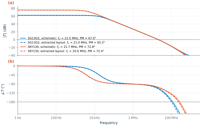
Table 16.2. Schematic against extracted layout (unity-gain buffer, CL = 2 pF, tt, 27 °C; slew rates from a 0.3 V step, 20–80 %).
| Quantity | SG13G2 schematic | SG13G2 layout | SKY130 schematic | SKY130 layout |
|---|---|---|---|---|
| DC loop gain | 62.2 dB | 62.2 dB | 75.7 dB | 75.7 dB |
| Unity-gain frequency | 21.5 MHz | 21.0 MHz | 21.7 MHz | 20.6 MHz |
| Phase margin | 67.0° | 65.3° | 72.8° | 72.4° |
| Slew rate, rising / falling | 17.0 / 15.6 V/µs | 17.0 / 14.7 V/µs | 16.5 / 14.6 V/µs | 16.0 / 13.7 V/µs |
| Overshoot of the 0.3 V step | 0.27 % | 0.58 % | 0.14 % | 0.22 % |
| Offset | −0.13 mV | −0.13 mV | −0.09 mV | −0.09 mV |
The DC quantities do not move, because the extraction adds capacitance and no resistance. Everything that depends on capacitance moves a little in the expected direction. In SKY130 the 43 fF across \(C_c\) raises the compensation capacitance by about 4 %, and the unity-gain frequency, \(g_{m1}/(2\pi C_c)\), falls by 5 %. In SG13G2 the extra capacitance sits mostly on the first-stage output and the output, where it lowers the non-dominant pole: the phase margin falls by 1.7°. The falling slew rate, set by the current that charges \(C_c\) and the output, drops by 6 % in both. The design keeps all its specifications with margin, which is what the margins of Chapter 12 were for. Lab 8 runs exactly this comparison.
What this means for your design
Design with margin for the parasitics you cannot see in the schematic, then measure them. A 5 % margin on bandwidth and a few degrees on phase margin are enough for a compact block like this one; a block with long routes, a large capacitor array or a wide bus needs more. Look at the largest extracted capacitors first: they tell you which wire to shorten, which capacitor to move or which node to shield. And repeat the corner sweep of Section 12.8 on the extracted netlist before you trust the margins at the corners.
16.6 Fill, density and antennas
The checks so far were on the block. Before tape-out the block sits in a chip, and three chip-level checks of Chapter 17 apply to it.
Density. The OTA alone is far from the density windows. In SG13G2 its active area covers 18 % of its bounding box and its metals 1 to 11 % (Metal1 6 %, Metal2 8 %, Metal3 2 %, Metal4 1 %, Metal5 11 % because of the MIM bottom plate), against the 35 % minimum for active and metals of Table 17.1; in SKY130 the diffusion covers 15 % and met1 to met4 4 to 19 %. Fill shapes added at chip level bring every window into range, with exclusion areas over the input pair and the MIM capacitor. After fill, extract and simulate again: fill near a node adds capacitance that this chapter’s extraction has not seen.
Antennas. The SG13G2 antenna rules, which run_drc.py checks only on request, report no violations for this block: its input-pair gates are large (each finger 4.55 × 3 µm), and the long routes run on Metal3 spines that reach the gates through short Metal2 tracks. In a chip, the wire from a pad to an input gate is the one to watch (Worked example 17.1).
The top cell. DRC and LVS are repeated on the complete top cell with pads, seal ring and fill. The block results of Table 16.1 are necessary, not sufficient.
Try it · Lab 8
Lab 8 runs this chapter’s flow on the course OTA in your PDK, then breaks the layout on purpose (a missing via, a shorted net, a dummy left out of the reference) and asks you to find each error from the reports.
- DRC checks geometry against the rule deck, LVS checks that the drawn circuit is the schematic’s, and extraction gives the netlist for post-layout simulation. All three run in batch mode in IIC-OSIC-TOOLS;
tools/layout/verify.pyruns them for the course OTA.- The course OTA passes DRC (0 violations in the SG13G2 deck, its antenna rules and the SKY130 KLayout deck) and LVS in both PDKs. Magic’s full SKY130 rule set flags rpm.1 on the PDK resistor cell itself: understand such a report, cross-check it with the other deck and record it.
- The LVS reference must describe what is drawn (PDK passives, dummies) in the form the tool reads: IHP’s KLayout deck reads CDL-style
M/R/Clines and silently reads subcircuit-style lines as an empty schematic.- Magic finds 169 fF (SG13G2) and 144 fF (SKY130) of wiring capacitance. With it, the OTA loses 2.3 % and 4.9 % of bandwidth and 1.7° and 0.5° of phase margin; the DC gain and offset do not change.
- The block alone is far below the density windows (18 % active in SG13G2, 15 % in SKY130); fill, antenna and top-level checks follow at chip level, and the post-fill block must be extracted and simulated again.
Further reading
- The KLayout documentation on DRC, LVS and the netlist browser [39]: how a deck is written, and how to read a cross-reference.
- The Magic and Netgen documentation [40, 41]: extraction styles,
ext2spiceoptions and the Netgen setup files. - A. Hastings, The Art of Analog Layout [60]: verification from the layout designer’s side, and how to avoid the errors these tools find.
- The IHP SG13G2 layout rules [16]: the rule names that appear in the DRC reports, with figures.