Chapter 30
Assembling the Die
The last step turns blocks into a chip: estimate its area, plan its floor, build its pad ring, route its power and signals, and check it against a list of everything that goes wrong at tape-out. This chapter does all of it with the layouts of the earlier chapters and the pad cells the two PDKs ship, and ends with the course OTA assembled into a complete die in SG13G2 and in SKY130, pad ring and seal ring included, checked by each PDK's rule deck.
- Estimate die area from a block list before any layout exists, and calibrate the estimate against real layouts.
- Floorplan a mixed-signal die around noise, heat and matching, and decide whether it is limited by its pads or by its core.
- Build a pad ring from each PDK’s I/O cells, with power, ground and ESD for each domain, inside the seal ring of a shuttle.
- Size top-level power distribution from an IR-drop budget and the electromigration limits, and route sensitive signals.
- Run a final layout review from a checklist, and assemble and verify a real test chip.
Contents
The earlier chapters of this part drew devices and blocks. A foundry accepts neither: it accepts a die, a single top cell with a seal ring around its edge, bond pads that a wire can reach, protection on every pin, power that reaches every transistor, and a layout that passes the full rule deck (Chapter 17 listed what a submission must contain; Chapter 16 showed how DRC and LVS work). This chapter is about the steps in between: how big the die will be, where each block goes, what the pad ring is made of in each PDK, how wide the supply wiring must be, and how to check the result. The layouts come from the PDKs’ own cell libraries and generators in IIC-OSIC-TOOLS [35, 14, 20], assembled with KLayout’s Python API [39]:
python3 tools/layout/ch30/assemble_die.py        # survey of existing layouts, bond pad and seal rings, both test chips, 3D model
python3 tools/layout/ch30/assemble_die.py drc    # KLayout DRC of both complete dies (about two minutes)
python3 tools/figs/ch30_die.py                   # area estimate, floorplan, IR drop, figures and ch30_numbers.json
30.1 Estimating die area
Three parts of a die
A wire-bonded die has three parts. The core holds the circuits. The pad ring around it holds the I/O cells: bond pads, their ESD protection and the supply rails that run around the die (Chapter 29). The edge holds the seal ring and the space the bonding and sawing need. The die area is set by whichever of the first two is larger, plus the edge, and the estimate is worth making before any layout exists: it fixes the cost of a shuttle run (priced per square millimetre in Chapter 17), the package and the floorplan. With a well-partitioned design and factors calibrated on earlier layouts, it can be made surprisingly accurate [61].
Device areas by hand
Each device type has a simple area model. The parameters come from the PDK; the empirical factors come from layouts, and Part VII has plenty of those.
Key equation · Device areas for an estimate
\[A_R \approx \frac{R}{R_\square}\,w\,(w+s)\,k_R, \qquad A_C \approx \frac{C}{C''}\,k_C, \qquad A_{MOS} \approx n_u\left[n_f L + (n_f+1)\,s_{sd}\right] W_f. \tag{30.1}\]A resistor of \(R/R_\square\) squares of width \(w\), drawn as a serpentine with spaces \(s\), plus a factor \(k_R \approx 1.2\) for heads and dummies; a capacitor of density \(C''\) with a factor \(k_C\) for its terminals, dummies and spacing; \(n_u\) generator units of \(n_f\) gate fingers of width \(W_f\) and length \(L\) between \(n_f + 1\) source and drain strips of width \(s_{sd}\) = contact + 2 × contact-to-gate spacing.
The MOS formula is the footprint of the active area of one generator unit (Chapter 23). With \(s_{sd}\) = 0.16 + 2 × 0.11 = 0.38 µm in SG13G2 and 0.17 + 2 × 0.055 = 0.28 µm in SKY130, it reproduces the units of the course OTA within 1 %: an SG13G2 mirror unit of four 2.82 µm × 5 µm fingers comes out at 61.8 µm² against 61.5 µm² drawn by the PyCell, a SKY130 unit of two 5 µm × 2 µm fingers at 24.2 µm² against 24.4 µm² drawn by Magic. The factors are less obvious, and the layouts of the earlier chapters calibrate them:
- Resistors. The ABBA array of Chapter 27 (ten
rppdunits of 2 × 10 µm, 13 kΩ) gives 360 µm² from Eq. (30.1) with \(s\) = 1 µm; the layout, with its jumpers and pins, takes 537 µm². Use \(k_R\) ≈ 1.8 for a matched array, 1.2 for a plain serpentine. - Capacitors. The binary-weighted array of the same chapter holds 16 units of 5 × 5 µm, 400 µm² of plate, in 3352 µm² (SG13G2) and 3491 µm² (SKY130): the unit pitch (8 × 10.2 µm for a 5 µm plate in SG13G2), the ring of 20 dummies and the routing spines make \(k_C \approx 8.5\). A single large MIM plate, such as the OTA’s compensation capacitor, needs only \(k_C \approx 1.1\). Small units are expensive.
- MOS capacitors for decoupling. The 10 × 10 µm SG13G2 MOS capacitor of Chapter 26 holds about 1.27 pF (the 12.7 fF/µm² of Chapter 17 over its 100 µm² gate) in a 142 µm² cell: 8.9 fF/µm² of layout. A SKY130 NMOS of two 5 × 5 µm fingers used the same way gives 4.65 fF/µm² of layout instead of 7.9.
- Bipolar transistors and ESD devices. Their area depends on rings and spacings, not on the emitter, so take it from a drawn example: the 8 : 1 PNP arrays of Chapter 28 take 1157 µm² (SG13G2) and 1143 µm² (SKY130) [61].
- Logic. Standard cells have fixed sizes: an SG13G2 NAND2 is 1.92 × 3.78 µm and a reset flip-flop (
dfrbpq_1) 12.96 × 3.78 µm; in SKY130’ssky130_fd_sc_hdlibrary they are 1.38 × 2.72 µm and 9.2 × 2.72 µm (dfrtp_1) [14, 20]. Divide the cell area by a placement utilization of about 0.7.
Worked example 30.1 · The area of the course OTA from its device list, checked against its layout
The devices of Table 15.4, dummies included, through Eq. (30.1):
Group SG13G2 SKY130 Mirror bank, 15 units 15 × (4 × 5 + 5 × 0.38) × 2.82 = 926 µm² 15 × (2 × 2 + 3 × 0.28) × 5 = 363 µm² Input pair, 6 units 6 × (2 × 3 + 3 × 0.38) × 4.55 = 195 µm² 6 × (1.5 + 2 × 0.28) × 5 = 62 µm² PMOS mirror, 6 units 6 × (2 × 0.5 + 3 × 0.38) × 3.33 = 43 µm² 6 × (0.5 + 2 × 0.28) × 5 = 32 µm² Second stage (24 × 0.5 + 25 × 0.38) × 3.33 = 72 µm² (12 × 0.5 + 13 × 0.28) × 5 = 48 µm² MOS total 1236 µm² 505 µm² Cc plate (1 pF) 25.8² = 666 µm² 22.2² = 493 µm² Against the layout. The three device groups of Figure 15.4, each with its guard ring, gate straps and Metal2 tracks, occupy 2743 µm² (SG13G2) and 1265 µm² (SKY130): 2.2 and 2.5 times the bare footprints. The block, with the capacitor, the resistor, the spines and the space the floorplan leaves, measures 118.8 × 56.6 = 6725 µm² and 58.9 × 66.4 = 3911 µm², another factor of 1.9 and 2.1 over the boxes it contains. In one line: block ≈ 3.5 × (MOS footprints + capacitor plates) in SG13G2 and 3.9 × in SKY130, whose generator draws a guard ring around every unit.
What it means. The gate area alone (1070 µm² and 390 µm²) would underestimate the block six to ten times. For a new analog block, sum Eq. (30.1) over its devices and multiply by about 3.5 to 4; the factor falls towards 2 for blocks dominated by large regular devices (a big capacitor, a power transistor) and rises for small, ringed, matched ones.
From blocks to a die
The core holds the blocks plus the space between them, which two factors capture: a packing factor \(k_p\) for imperfect fitting (1.1 to 1.2 for a few dozen blocks that were not drawn to fit together) and a routing factor \(k_r\) for top-level wiring (about 1.1 to 1.3, less when most wiring can run over the blocks on upper metals) [61]. The core must fit inside the pad ring, and the pad ring must hold the pads. With \(N\) pads of pitch \(p\), I/O cells of depth \(h\), corner cells of side \(c\) and an edge \(e\) (seal ring, gap and, in SG13G2, the bond pads outside the cells), the die side is the larger of two numbers:
Key equation · Core-limited or pad-limited
\[D_{core} = \sqrt{k_p k_r \sum A_i} + 2(h + e), \qquad D_{pads} = 2(c + e) + \left\lceil \frac{N}{4} \right\rceil p, \qquad D = \max(D_{core}, D_{pads}). \tag{30.2}\]Because \(c \approx h\) in both I/O libraries, a square die is pad-limited when \(\sqrt{k_p k_r \sum A_i} < \lceil N/4\rceil\,p\): when the core is narrower than one side’s row of pads.
The I/O libraries of Section 30.3 give \(p\) = 80 µm and \(h = c\) = 180 µm in SG13G2, and \(p\) = 75 µm, \(h\) = 198 µm and \(c\) = 200 µm in SKY130; our edges are \(e\) = 143.4 µm and 16 µm. Eight pads leave a core of only about 160 µm on each side between the rows in either PDK; sixteen pads leave 320 µm (SG13G2) and about 310 µm (SKY130, whose corner cells are 4 µm longer one way). Table 30.1 applies Eq. (30.1) to the mixed-signal test chip of Section 30.2.
Table 30.1. Area estimate of a small mixed-signal test chip, in µm², from layouts already in the repository where they exist and Eq. (30.1) otherwise (tools/figs/ch30_numbers.json).
| Block | Source of the estimate | SG13G2 | SKY130 |
|---|---|---|---|
| DUT: the course OTA | layout of Chapter 15 | 6 725 | 3 911 |
| Test buffer for the output pad | 1.5 × OTA | 10 088 | 5 866 |
| Bandgap reference | PNP array of Chapter 28 + 100 kΩ + OTA | 8 806 | 5 803 |
| 6-bit SAR ADC: capacitor DAC | array of Chapter 27 scaled to 64 units | 9 312 | 9 697 |
| SAR ADC: comparator, logic | 0.5 × OTA; 12 flip-flops + 60 NAND2 at 70 % | 3 363 + 1 462 | 1 955 + 751 |
| Bias generator | 50 kΩ + 8 mirror units | 2 209 | 1 134 |
| LDO regulator | 400 µm pass device (Chapter 29 density) + OTA | 7 146 | 4 332 |
| Decoupling, 2 × 100 pF | MOS capacitors of Chapter 26 | 22 369 | 42 967 |
| Sum | 71 480 | 76 416 | |
| Core, × 1.15 × 1.2 | 98 642 (314 µm side) | 105 454 (325 µm side) | |
| Die, 16 pads: pad ring / core | Eq. (30.2) | 967 / 961 µm | 732 / 753 µm |
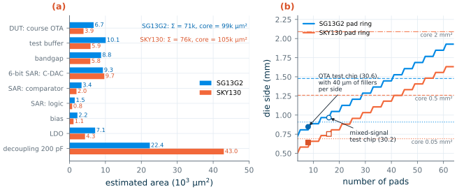
The estimate tells three things before a polygon is drawn. First, the 16-pad chip is balanced in SG13G2 (pad ring 967 µm, core 961 µm) but core-limited in SKY130, because its MOS decoupling capacitor, at half the density, takes 43 000 µm², more than half of the core. Second, the OTA itself is a small part of any of these dies. Third, a pad-limited die has free core area, and the best use of it is more decoupling capacitance, not looser layout.
Common pitfall · Estimating from the schematic’s W·L
The schematic lists W and L, and their product is the number most likely to be summed. It underestimates an analog block six to ten times (Worked example 30.1): every unit has contact strips, every group a ring, every matched device dummies, every capacitor array a dummy ring, and every block routing. Estimate from generator footprints and a calibrated factor, take arrays and bipolar devices from drawn examples, and do not forget the decoupling capacitance, which in a small analog chip is often the largest block of all.
30.2 Floorplanning
What goes where
A floorplan is a scaled sketch of the die: the outline, the pad ring with every pad named, and each block as a rectangle of its estimated area, with the main supply and signal routes drawn in. It is the cheapest place to fix a noise or matching problem, because nothing has been drawn yet. Five considerations decide it, roughly in this order [61]:
- The pads come first. The package or the test board fixes their order, and each block should sit next to its own pads. Put the supply pair of each domain on neighbouring pads, so that the two bond wires form a small loop (Chapter 17’s bounce), and the two inputs of a differential pair on neighbouring pads, so that whatever couples into them couples equally.
- Noise. Separate the aggressors (logic, clocks, output drivers, the switching regulator) from the victims (high-impedance analog nodes, references, the comparator input) by distance and by a guard ring (Chapter 29 found that injected electrons travel 55 to 175 µm), give them separate supply pads, and route no digital signal across an analog block.
- Heat. A block that dissipates (a regulator’s pass device, an output stage) makes a temperature field that is steepest close to it. Keep matched devices far from it and orient them so that the isotherms run along their axis of symmetry; Chapter 27 showed that a common centroid cancels the linear part of the gradient.
- Matching and stress. Packaging stress is largest at the edges and corners of the die. Put precision blocks (the bandgap’s bipolar array, the capacitor DAC, the input pair) in the inner part of the core, on the die’s axis of symmetry if possible.
- Signal flow. Arrange the blocks in the order the signal passes through them, so that routes are short and do not cross, and leave channels where the top-level wiring has to pass.
A mixed-signal test chip
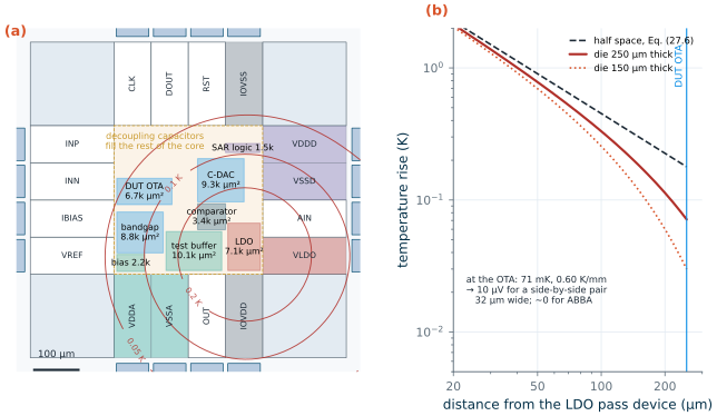
Figure 30.2a applies this to the chip of Table 30.1 in SG13G2, drawn to scale but as a sketch: the blocks are rectangles of the estimated areas, not layouts. Sixteen sg13g2_io cells fill the ring, four per side at 80 µm, which leaves a 320 µm square core. The analog supply pair (VDDA, VSSA) and the output sit on the south side, the DUT’s inputs, its bias and the reference output on the west, the digital pads (CLK, DOUT, RST, VDDD, VSSD) on the north and the upper east side, and the I/O supply pads at the eastern ends of the south and north rows. Inside, the DUT and the bandgap occupy the west half next to their pads; the SAR logic sits in the north-east corner with its pads; the capacitor DAC and comparator lie between them, the DAC in the inner core; the LDO, the only block that dissipates noticeably (20 mA from 3.3 to 1.2 V, 42 mW), sits in the south-east corner, as far from the DUT as the core allows, next to its own pad. Decoupling capacitors fill everything else.
Heat on a real die
Chapter 27 used the half-space formula, Eq. (27.6), for the temperature around a heat source. A real die is a slab a few hundred micrometres thick, glued to a package paddle that holds its bottom near a fixed temperature, with sides that lose little heat. Both boundaries can be written as image sources. The isothermal bottom at depth \(t\) mirrors the source with alternating sign at depths \(2nt\); the adiabatic sides mirror it with the same sign across each edge. For a source \(P\) at the surface and a point at lateral distance \(\rho_j\) from the \(j\)-th lateral image,
\[\Delta T = \frac{P}{2\pi k}\sum_j \sum_{n=-\infty}^{\infty} \frac{(-1)^n}{\sqrt{\rho_j^2 + (2nt)^2}}. \tag{30.3}\]The \(n = 0\) term of the source itself is Eq. (27.6). Close to the source the die looks like a half space; at distances comparable with \(t\) the bottom takes over and the field decays faster than \(1/r\). ch30_die.py sums Eq. (30.3) with \(k\) = 148 W/(m·K) and an assumed thickness of 250 µm (ask your shuttle for the real value after back-grinding; 150 µm is shown for comparison). At the DUT, 253 µm from the LDO, the half space predicts 178 mK; the finite die gives 71 mK and a gradient of 0.60 K/mm. Across the 32 µm of the OTA’s input pair that is 19 mK, 10 µV of offset for a side-by-side pair at −0.53 mV/K (Chapter 27), and essentially nothing for the ABBA pair the OTA actually uses. The sides matter mostly near the die edge, where they double the local rise.
What this means for your design
In a small, low-power test chip, heat is rarely the problem: a 42 mW block a quarter of a millimetre away costs a common-centroid pair nothing measurable. Noise and supply drops are the problems, and the floorplan solves them by distance, by separate supply pads and by keeping digital routes out of analog blocks. Spend the floorplan’s effort there, put the matched blocks in the inner core, and treat any block above about 100 mW as a thermal design problem of its own.
30.3 The pad ring
What a pad ring is made of
A pad ring is built from a few kinds of cells that abut along the edge of the die (Figure 30.3):
- Pad cells, one per pin: a signal pad (analog, input, output, bidirectional) or a supply pad. Each holds the ESD devices of its pin, diodes to the rails for a signal pad and an RC-triggered rail clamp for a supply pad (Chapter 29), and the bond pad itself or the connection to it.
- Corner cells, which turn the rails around the corners.
- Filler cells, which carry the rails across gaps between pads; some PDKs add cells that join or split rails between supply domains.
- The rails: wide metal rings, stacked on several layers, that every cell contains at the same position, so that abutting cells connect them. They carry the I/O supply, the core supply and the ESD current around the whole die.
- The seal ring and the edge space between the bond pads and the saw line (Chapter 17).
Table 30.2 compares the two libraries as IIC-OSIC-TOOLS 2026.10 ships them; the dimensions come from their LEF and GDS files and the seal rings from the PDKs’ generators [14, 20, 18].
Table 30.2. The I/O libraries and die edges of the two PDKs.
| Quantity | SG13G2 (sg13g2_io) |
SKY130 (sky130_ef_io, wrapping sky130_fd_io) |
|---|---|---|
| Pad cell, width × depth | 80 × 180 µm | 75 × 197.965 µm (analog_esd_pad 75 × 200) |
| Corner cell | 180 × 180 µm | 200 × 204 µm |
| Fillers | 1, 2, 5, 10, 20, 50 µm (Filler200 … Filler10000) |
1, 5, 10, 20 µm (com_bus_slice_*) |
| Signal pads | analog (with 587 Ω secondary protection), input, output 4/16/30 mA, tri-state, bidirectional | analog with 5 + 5, 1 + 1 or no diodes, GPIO (gpiov2) |
| Supply pads | IOPadVdd, IOPadVss (core), IOPadIOVdd, IOPadIOVss (3.3 V I/O) |
VCCD/VSSD (1.8 V), VDDA/VSSA (analog), VDDIO/VSSIO (3.3 V), each with or without clamp (*_clamped_pad) |
| Rails in every cell | vdd, vss, iovdd, iovss (Metal3–TopMetal2) | VCCD, VSSD, VDDA, VSSA, VDDIO, VSSIO, VDDIO_Q, VSSIO_Q, VCCHIB, VSWITCH, two analog buses (met4, met5) |
| Domains | one core and one I/O domain per ring (no splitting cell) | split with disconnect_vdda/vccd_slice_5um, tie with connect_*_slice_20um |
| Bond pad | not in the cell: the assembler adds it outside (IHP PyCell bondpad, 70 × 70 µm here) |
inside the cell, 60.8 µm of met5, its edge about 34 µm from the outer edge |
| Seal ring | PyCell sealring: EdgeSeal 4.2 µm wide, 25 µm edge box with passivation ring (Seal.a ≥ 3.5 µm) |
open_pdks generator: advSeal_6um_gen, 6 µm |
| Pad rules | width 30–150 µm, space ≥ 8.4 µm, 25 µm to the EdgeSeal for wire bonding (Pad.aR, a1, bR, dR) | pad space ≥ 1.27 µm (pad.2 in the KLayout deck) |
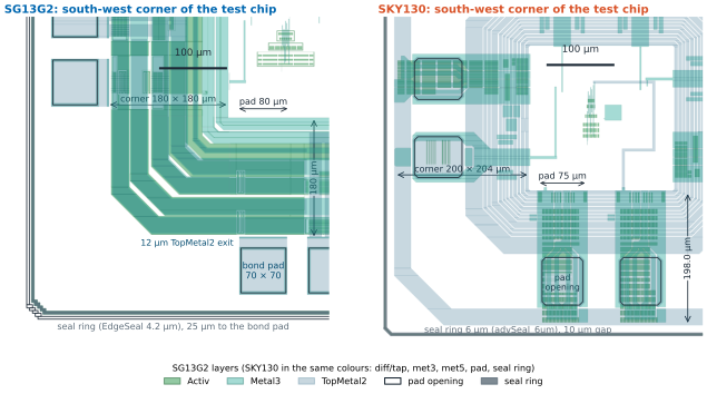
tools/layout/ch30/assemble_die.py.Two differences in Table 30.2 shape every SG13G2 and SKY130 floorplan. The SG13G2 cells leave the bond pad to the designer, and the pad rules then push the die outwards: a 70 µm pad, a short exit, 25 µm to the seal ring (Pad.dR) and the 25 µm edge box of the seal ring itself add 143 µm on every side, so that a minimal SG13G2 ring with two pads per side already needs a 0.81 mm die. The SKY130 cells contain their pads and many more rails, because SkyWater’s ring was designed for chips with several analog and digital domains, such as the Caravel harness below, and a chip that uses fewer domains must still tie the unused rails somewhere.
Supply pads, domains and clamps
How many supply pads does a domain need? Four limits apply; take the largest count:
- Current. Each supply pad and its bond wire carry a share of the domain’s current. With the electromigration limits of the rails and of the bond wire (the bond wire of Chapter 17 has about 0.1 Ω per millimetre), a few tens of milliamperes per pad is a comfortable figure for these cells; Section 30.4 computes the drop.
- Bounce. The inductance of the supply bond wires sets the bounce of Chapter 17; \(n\) pads in parallel divide it by roughly \(n\), as long as their wires are not coupled.
- ESD. The rail clamps sit in the supply pads (SG13G2’s
IOPadVddandIOPadIOVdd, SKY130’s*_clamped_padcells), and Chapter 29 showed that the ESD current crosses the rail from the stressed pad to the nearest clamp: about one ohm of rail costs two volts at 2 kV HBM. On a long ring, add supply pads (or clamp cells) so that no pad is far from a clamp, and keep the rails unbroken. - Domains. Each domain needs at least one VDD and one VSS pad, and the ESD network must also protect between domains: a discharge from a VDDA pad to a VSSD pad crosses from one ground to the other. Domains that share the substrate are joined by back-to-back diodes between their grounds, or by a common ground rail, so that the ESD current has a path [61, 70].
In SKY130 this is what the slice cells are for. A disconnect_vdda_slice_5um breaks the VDDA and VSSA rails between two parts of the ring, so that each part can carry its own analog domain; the connect_*_slice_20um cells tie rails together, VDDA to VDDIO and VSSA to VSSIO, or VCCHIB to VCCD and VSWITCH to VDDIO, which a chip with only one 1.8 V and one 3.3 V domain needs so that no rail floats. Our SKY130 test chip uses both connect slices. The SG13G2 library has no splitting cell: its ring carries one core domain and one I/O domain, so a separate analog core supply in SG13G2 needs its own rails inside the core or a ring built with breaks and protection of its own.
Shuttle frames
On a shared die, the frame is given. Chapter 17 described the routes; here are the dimensions a floorplan needs:
- IHP Open-Silicon MPW (SG13G2). You deliver a complete die of any size, with your own pad ring and seal ring, priced per square millimetre [25]. The frame is therefore the one of Table 30.2: 80 µm pad pitch with
sg13g2_io, bond pads of 30–150 µm at least 8.4 µm apart, 25 µm from the pad opening to the seal ring, and the seal-ring PyCell [16]. - Caravel harness (SKY130, ChipFoundry). The pad ring, seal ring, management core and power pads are fixed; the user project area is 2.92 × 3.52 mm and reaches the outside through 38 I/O pads and 4 power pads [34]. Analog pins pass through the
sky130_ef_ioanalog pads at the harness’s fixed pad positions. ChipFoundry quotes up to 15 mm² of user area for its current chipIgnite service (Chapter 17), so check the frame of your run. - Tiny Tapeout (both PDKs). A tile of 160 × 225 µm or 334 × 225 µm inside someone else’s die; the pad ring and its protection belong to the shuttle, and an analog pin brings up to 500 Ω and 5 pF of its own (Chapter 17) [47].
SG13G2 vs SKY130 · Pad rings you can build
SG13G2 SKY130 Minimal die, 8 pads (two per side) 0.81 mm (0.85 mm with our 200 µm core) 0.59 mm (0.64 mm with our 214 µm core) Edge per side, outside the I/O cells 143.4 µm: seal ring 36.4, gap 25, exit 12, bond pad 70 16 µm: seal ring 6, gap 10 (our choice) Pad pitch 80 µm 75 µm Rails per cell 4 12 (2 of them analog buses) Pads for one analog core VDD, VSS, IOVDD, IOVSS VCCD, VSSD, VDDIO, VSSIO, plus connect slices In SG13G2 you build the whole frame, including the bond pads and the seal ring, from the PDK’s cells and PyCells. In SKY130 the cells are complete but complex; outside a full-die run you will usually sit inside the Caravel harness or a Tiny Tapeout tile, whose ring is already built and verified.
30.4 Top-level routing and power distribution
Power, from the bond wire to the transistor
The supply voltage that reaches a block is the pad voltage minus four drops in series: the bond wire and pad, the ring between the supply pad and the point where the block’s grid joins it, the grid across the core, and the block’s own wiring. Each is a resistor carrying part of the current, and each has a hand formula.
A power grid of stripes of width \(w\) at pitch \(p\) in each direction behaves, seen from far away, like a sheet with an effective sheet resistance \(R_{eff} = R_\square\,p/w\) per direction. A core of side \(a\) that draws a uniform current density \(J\) and is fed from a ring on all four sides has a drop \(U(x, y)\) that obeys the Poisson equation \(\nabla^2 U = -J R_{eff}\), and its maximum for a square is a standard result:
Key equation · Drop in a power grid and its ring
\[\Delta V_{grid} \approx 0.0737\,J R_{eff}\,a^2 \ (\text{fed on four sides}), \qquad \tfrac18 J R_{eff}\,a^2 \ (\text{two sides}), \qquad \Delta V_{ring} \approx \frac{I}{n}\,\frac{R'_{ring}\,s}{8}. \tag{30.4}\]\(R_{eff} = R_\square p/w\); with different layers in \(x\) and \(y\), use the geometric mean, or the two-sided formula with the lower of the two when they differ several times. The ring term assumes \(n\) supply pads spaced \(s = 4a/n\) apart along a ring of resistance \(R'_{ring}\) per unit length, with the current entering it evenly.
Derivation · Where 0.0737 and 1/8 come from
Fed from two opposite edges, the problem is one-dimensional: \(U'' = -JR_{eff}\) with \(U = 0\) at \(x = 0\) and \(x = a\) gives \(U = \tfrac12 JR_{eff}\,x(a - x)\), largest at the centre, \(JR_{eff}a^2/8\). Fed from all four edges, \(U = JR_{eff}a^2\,u(x/a, y/a)\) with \(\nabla^2 u = -1\) in the unit square and \(u = 0\) on its edges. Expanding \(u\) in the eigenfunctions \(\sin(m\pi x)\sin(n\pi y)\), odd \(m\) and \(n\), gives
\[u\left(\tfrac12, \tfrac12\right) = \frac{16}{\pi^4}\sum_{m,n\ \mathrm{odd}} \frac{(-1)^{(m+n)/2-1}}{mn\,(m^2 + n^2)} \approx 0.0737.\]The ring term is the one-dimensional result again: a ring segment of length \(s\) between two pads, fed at both ends, collecting \(I/n\) evenly along its length, has its largest drop \((I/n)(R'_{ring}s)/8\) in the middle. If the grid delivers its current to the ring mostly near the pads, as it does when the pads sit at the middle of the sides, the true ring drop is smaller.
Worked example 30.2 · The supply drop of a 1 mm core drawing 50 mA, by hand and by network
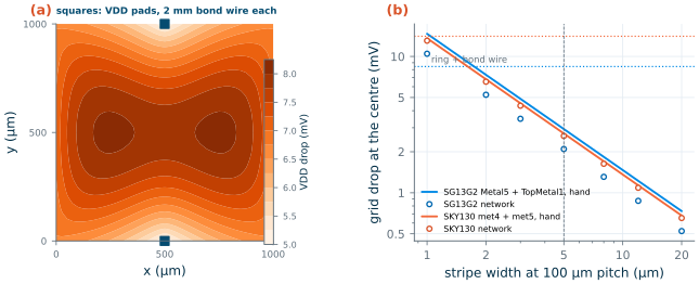
A 1 × 1 mm core draws 50 mA evenly (\(J\) = 50 mA/mm²). Each net has 5 µm stripes every 100 µm in both directions, on the two metals below the top one; a 20 µm ring on the top metal; two VDD pads at the middles of two opposite sides, each with a 2 mm bond wire of 0.2 Ω (Chapter 17). Sheet resistances from Table 15.3.
SG13G2. Metal5 stripes in \(x\): \(R_{eff}\) = 0.088 × 20 = 1.76 Ω; TopMetal1 in \(y\): 0.018 × 20 = 0.36 Ω. Geometric mean 0.796 Ω: \(\Delta V_{grid}\) = 0.0737 × 0.05 A/mm² × 0.796 Ω × 1 mm² = 2.93 mV. The two directions differ five times, so most current flows along TopMetal1 to the north and south edges: the two-sided formula with 0.36 Ω gives 2.25 mV. Ring on TopMetal2: \(R'\) = 0.011/20 = 0.55 mΩ/µm, \(s\) = 2 mm, \(\Delta V_{ring}\) = 25 mA × 1.1 Ω / 8 = 3.44 mV. Bond wire: 25 mA × 0.2 Ω = 5.0 mV. Total by hand 10.7 to 11.4 mV.
SKY130. met4 in \(x\): 0.047 × 20 = 0.94 Ω; met5 in \(y\): 0.58 Ω; mean 0.738 Ω: 2.72 mV (two-sided with 0.58 Ω: 3.63 mV). Ring on met5: \(R'\) = 1.45 mΩ/µm, 9.06 mV. Bond wire 5.0 mV. Total by hand 16.8 mV.
The network.
ch30_die.pysolves the stripe network node by node. With an ideal ring the grid drop is 2.09 mV (SG13G2) and 2.61 mV (SKY130): the square formula is right within 4 % when the two directions are similar (SKY130) and the two-sided one within 8 % when one direction dominates (SG13G2). With the resistive ring and the bond wires the total is 8.0 mV and 10.3 mV: the hand ring term is pessimistic because the grid delivers most of its current to the ring near the pads. That is 0.67 % of 1.2 V and 0.57 % of 1.8 V, and the VSS network adds the same again.Electromigration. The busiest stripe carries \(J\,p\,a/2\) = 2.5 mA where it meets the ring: 1.25 µm of Metal5 or met4 at 2 mA/µm, 0.17 µm of TopMetal1, 0.83 µm of met5 (Table 24.2). The ring next to a pad carries 12.5 mA in each direction: 0.78 µm of TopMetal2, 4.2 µm of met5. At 125 °C divide by 0.54. In a grid sized for 1 % drop, electromigration is not the limit; in the thin connections into the blocks it can be.
For the course OTA the same arithmetic is short. It draws 93 µA (Chapter 12); the 300 µm VDD route of the SG13G2 test chip, 4 µm of Metal5, is 6.6 Ω and drops 0.6 mV; the SKY130 route on met5 drops 0.2 mV. An analog block’s supply route is sized by what shares it, not by the block: the same route shared with a 5 mA digital block would drop 33 mV and carry that block’s switching noise into the OTA, which is why each sensitive block gets its own route back to its own pad, joining the others only at the pad (a star connection) [61].
Widths and cuts from electromigration
Table 30.3 turns the limits of Table 24.2 into the width and the number of cuts that 10 mA needs; scale linearly for other currents.
Table 30.3. Minimum width and cut count for 10 mA DC, at 105 °C (Table 24.2) and at 125 °C (× 1/0.54). SKY130 values are the estimate of Chapter 24, not foundry numbers.
| SG13G2 layer or cut | 105 °C | 125 °C | SKY130 layer or cut | 105 °C | 125 °C |
|---|---|---|---|---|---|
| Metal1 | 10.0 µm | 18.5 µm | met1, met2 | 11.7 µm | 21.6 µm |
| Metal2–Metal5 | 5.0 µm | 9.3 µm | met3, met4 | 5.0 µm | 9.2 µm |
| TopMetal1 | 0.67 µm (min. 1.64) | 1.23 µm (min. 1.64) | met5 | 3.3 µm | 6.2 µm |
| TopMetal2 | 0.62 µm (min. 2.0) | 1.16 µm (min. 2.0) | |||
| Via1–Via4 | 25 cuts | 47 cuts | via; via2, via3 | 40; 23 cuts | 75; 43 cuts |
| TopVia1; TopVia2 | 8; 1 cuts | 14; 2 cuts | via4 | 2 cuts | 3 cuts |
Wide supply metal has two more rules. SG13G2 requires slits in any metal wider than 30 µm (Slt.c, slits 2.8 to 20 µm wide), to relieve the mechanical stress of a large plate [16]; run the slits along the current, so that they cost little resistance, and split a wide bus into parallel stripes of less than 30 µm instead. And where a wide bus changes layer, fill the whole overlap with cuts: a single column of vias at the edge of an overlap carries most of the current in its first few cuts [61].
Signals across the die
Most top-level analog signals carry little current; what matters is what couples into them. A wire next to an aggressor forms a capacitive divider: a step \(\Delta V_a\) on the aggressor moves a floating victim node by
\[\Delta V_v = \frac{C_c}{C_c + C_v}\,\Delta V_a, \tag{30.5}\]where \(C_c\) is the coupling and \(C_v\) the victim’s capacitance to everything else. A driven node recovers with the time constant of its driving resistance and \(C_v\); a high-impedance node (a sampled voltage, a comparator input, a bias line from a large resistor) keeps the error. Magic’s SKY130 extraction file gives the sidewall coupling between two met2 wires as 50 aF per micrometre of length at its reference spacing [20]: 100 µm of parallel run couples about 5 fF, and a 1.2 V clock edge then moves a 100 fF bias node by 57 mV. Hence the rules of top-level routing [61]:
- Separate by distance and by layer. Coupling falls quickly with spacing. Cross aggressors at right angles; never run them in parallel with a sensitive line.
- Shield. A grounded wire between two lines, or a grounded plane between two layers, sends the coupling to ground instead of the victim; the shield must return to the victim’s own ground (Chapter 25 shielded resistors the same way).
- Route differential signals as pairs, side by side and the same length, so that whatever couples does so in common mode.
- Slow the edges of static control lines with a series resistor, and route all digital lines in a digital channel that does not cross analog blocks.
- Keep Kelvin connections Kelvin. A sense line that joins a force line anywhere but at the point to be measured measures the drop of the force line too.
30.5 The final layout checklist
A last review before tape-out catches what the tools do not check. The list below is ours; it assumes that the steps of Chapter 16 and the submission flow of Chapter 17 (Figure 17.6) have been run, and asks what is still easy to miss. Each item should have an answer someone can show.
The evidence
- Full DRC of the final top cell, with fill, density and antenna checks on, is clean, and every remaining marker has a written reason that the foundry has accepted. A clean block DRC is not enough.
- LVS of the top cell, pads included, matches, and so do the device parameters, not only the connectivity.
- Post-layout simulation of the top cell includes the pads, the bond wires and the extracted wiring, at the corners and temperatures of the specification.
The die and the ring
- Every pin of the package or board has a pad, in the order the bonding diagram expects; unused inputs are tied.
- Each supply domain has enough VDD and VSS pads for its current, its bounce and its ESD (Section 30.3), adjacent to each other.
- The ring is unbroken except where a domain split is intended, and every split has a protection path between the domains.
- The seal ring is the PDK’s own, there is exactly one, and nothing lies outside it; bond pads keep their distance to it.
Power and current
- Each supply route has a computed drop and a computed current density, at the hottest temperature, including the vias at every layer change (Table 30.3).
- Sensitive blocks have their own supply routes back to their pads; no digital current flows in an analog ground.
- Wide metal follows the slit rules, and stress slits run along the current.
Signals, matching and noise
- No aggressor runs in parallel with a high-impedance node; crossings are at right angles or shielded.
- Matched devices sit in the inner core, away from the die edge, the pads and any block that dissipates; their surroundings and routes are symmetric (Chapter 27).
- Fill does not land on matched devices or capacitor arrays unless it is the PDK’s matched fill; fill-exclusion areas are drawn where needed.
Reliability and protection
- Every pad has its ESD path, and the resistance from each pad to the nearest clamp is known (Chapter 29); gates connected to a pad have secondary protection close by.
- Junctions that a pin can forward-bias have guard rings, and latch-up rules hold near every I/O cell (Chapter 24).
- Antenna diodes or jumpers protect the long top-level routes that end on gates.
The hand-off
- Top cell name, layer map, cell names unique against other designs on the shuttle, no unresolved references, a die size that matches the booking.
- The archive holds the GDS, the scripts that made it, the decks and tool versions used, the schematics and the simulation results, with checksums. For an open design, the repository is the archive; tag the commit you submitted.
30.6 A test chip for the course OTA
What the script builds
assemble_die.py turns the Chapter 15 OTA into a complete die in both PDKs. It places the PDK’s I/O cells, corners and fillers around a square, eight pads in all, two per side: the two inputs on the north side, the core supply pair on the south side, the bias and the output on west and east, and the I/O supply pads, which power the pads’ ESD diodes, on west and east as well. In SG13G2 it adds the bond pads outside the cells (IHP PyCell bondpad, 70 × 70 µm) and the seal-ring PyCell; in SKY130 the two connect slices on the west side and open_pdks’ seal ring. The OTA goes in the centre, and Manhattan routes on Metal3/met3 and Metal4/met4 join its pins to the pads, with VDD carried around the block on Metal5/met5. The inputs connect to the protected padres node of the SG13G2 analog pad, so that their gates have the secondary protection of Chapter 29 (at the cost of 587 Ω of thermal noise, 3.1 nV/√Hz, from Chapter 17); the output and bias use the direct pad node. The script checks that no two nets touch on the same layer and that no route enters the OTA except at its pins. It writes only what we draw; the I/O cells, the OTA, the bond pad and the seal ring are references that are filled from their libraries when the die is verified or rendered.
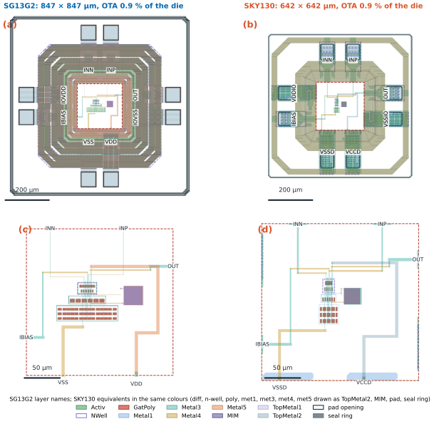
sg13g2_io ring, bond pads, seal ring. (b) SKY130, 642 µm square: sky130_ef_io ring and seal ring. Red dashed: the core inside the rings. (c, d) The cores with the routes from the OTA's pins to the pads (labels at the pad ends). Layouts from the PDK libraries and the Chapter 15 GDS, assembled by tools/layout/ch30/assemble_die.py; DRC results in the text.The numbers are those of a pad-limited chip (Figure 30.1b). The SG13G2 die is 846.8 µm square, 0.717 mm², of which the OTA’s 6725 µm² is 0.94 %; at the €2800 per mm² of IHP’s run it would cost about €2000, of which €19 pays for the amplifier. The SKY130 die is 642 µm square, 0.412 mm², with the OTA at 0.95 %. The cores between the rings are 200 µm (SG13G2, where we added 40 µm of fillers per side for room to route) and 214 µm (SKY130) square.
The northern part of the SG13G2 test chip around the INN pad: OTA, routes, I/O cell, exit and bond pad (contacts and vias omitted); 270 kB.
Verification
Both dies were checked with the full KLayout decks of the PDKs, without the density checks, because neither chip has fill yet [16, 20]:
- SG13G2: zero violations on the complete die (IHP
run_drc.py, 90 s). The first assembly placed the bond pads directly against the I/O cells and the deck answered with 153 markers, all of them recommended rules: Pad.fR (a metal exit from the pad at least 7 µm long) on Metal2 to TopMetal2, and Pad.d1R (11.2 µm from the pad to active devices). A 12 µm TopMetal2 exit between each cell and its pad cleared them, at the price of 24 µm of die width. - SKY130: nine violations of m5.2 (met5 spacing, 1.6 µm), all inside SkyWater’s own cells:
sky130_fd_io__top_power_lvc_wpadandsky130_fd_io__overlay_vccd_lvc, the core of the 1.8 V clamped supply pads, where two met5 shapes on the cell’s core edge are 1.1 µm apart. None comes from our routes or the OTA. A shuttle that uses these cells waives them; check with your provider.
What was not done, and would be before a tape-out: fill and the density checks, the antenna check, LVS of the top cell against a netlist with the pad cells, and a post-layout simulation with the pads and bond wires. The SKY130 deck was run without its seal-ring checks, as in the other chapters.
Try it · Your own test chip
In
tools/layout/ch30/assemble_die.py, the dictionariesSGandSKdescribe each ring. Changerowsto three pads per side and add the pads you want topads(for example a second VSS pad next to the first,("VSS2", "sg13g2_IOPadVss")), then runpython3 tools/layout/ch30/assemble_die.py gen build export drcandpython3 tools/figs/ch30_die.py testchip: how much larger is the die, and is it still pad-limited? Setbp_exitback to 0 and watch the recommended pad rules return. Intools/figs/ch30_die.py, move the LDO infloorplan_geometry()next to the DUT and rerunpython3 tools/figs/ch30_die.py floorplan; then changeW_GRIDorW_RINGand rerunirdropto find the narrowest grid that keeps Worked example 30.2 below 1 % of VDD.
The end of Part VII
This chapter closes the part that began with a mask and a rule. Chapter 23 explained what each drawn layer becomes and why each rule exists; Chapter 24 added the slow ways a chip fails: electromigration, latch-up and antennas. Chapters 25 to 28 drew the devices an analog designer uses (resistors, capacitors and inductors, matched arrays, bipolar transistors and diodes), and Chapter 29 the large devices and the protection every pin needs. Here they came together in a die. The same pattern ran through all of it: a physical effect, a number from the PDK, a hand estimate, a layout from the PDK’s own generators, and a check by the PDK’s own deck, in two processes side by side. A real chip adds fill, LVS and a measurement, which Chapters 16 and 17 cover; everything else on the way from a schematic to silicon is now in the course.
- Estimate die area from generator footprints, not W·L: the course OTA’s block is 3.5 (SG13G2) and 3.9 (SKY130) times its MOS footprints plus capacitor plates; take arrays, bipolar devices and decoupling from drawn examples.
- The die is the larger of the core and the pad ring, Eq. (30.2). With 80 µm (SG13G2) or 75 µm (SKY130) pads, a small analog chip is pad-limited; the 16-pad chip of Table 30.1 is balanced in SG13G2 and core-limited in SKY130, where decoupling takes half the core.
- Floorplan from the pads inward: supply pairs and differential inputs on neighbouring pads, aggressors in one corner, matched blocks in the inner core. A 42 mW block 250 µm away costs a common-centroid pair nothing measurable; the die’s bottom halves the half-space estimate.
- SG13G2’s
sg13g2_ioring has four rails and leaves bond pad and seal ring to you (143 µm of edge per side, 0.85 mm for the eight-pad chip); SKY130’ssky130_ef_ioring has twelve rails, pads inside the cells and slices to split or tie domains.- Budget the supply drop as bond wire + ring + grid + local route, Eq. (30.4): for a 1 mm, 50 mA core the network gives 8.0 mV (SG13G2) and 10.3 mV (SKY130), with the bond wire the largest term; electromigration sizes the thin connections, not the grid.
- The OTA test chips pass DRC with zero violations (SG13G2) and nine violations inside SkyWater’s own power-pad cells (SKY130); fill, antenna, top-level LVS and post-layout simulation remain before a tape-out.
Further reading
- R. A. Hastings, The Art of Analog Layout [61]: Chapter 15 (die-area estimation, floorplanning, the pad ring with scribe streets, seal rings and bond pads, top-level interconnection and a final layout checklist), the source of the scope of this chapter.
- The I/O libraries themselves:
sg13g2_iowith its README and the IHP layout rules for pads and seal rings [14, 16], andsky130_fd_iowith SkyWater’s documentation and thesky130_ef_iowrappers of open_pdks [18, 20]. - The Caravel harness repository [34]: a complete SKY130 pad frame with several analog and digital domains, the best example of the slice cells in use.
- IHP’s Open-Silicon MPW page [25] and Tiny Tapeout’s analog specification [47]: the frames, prices and pin limits of the routes to silicon that this course uses.