Chapter 17
Fabrication, Packaging and Tape-Out
Hundreds of process steps turn your GDS file into transistors and wires. Knowing them explains the design rules you have been obeying, the package adds parasitics that your simulation never saw, and open shuttles now let a student send a design to a real fab and measure it.
- Follow a 130 nm CMOS wafer through the main front-end and back-end process steps, and relate each step to a design rule.
- List what a foundry needs at tape-out: a DRC-clean GDS with fill, density, antenna and seal-ring rules met, and a clean LVS.
- Describe the pad ring, the ESD cells of each PDK and the package, and estimate the supply bounce caused by bond-wire inductance.
- Compare the routes to silicon open to SG13G2 and SKY130 designers in November 2026, with their costs and schedules.
- Plan the measurement of the course-project OTA and compare it fairly with simulation.
Contents
17.1 From wafer to chip
When you tape out a design, you send the foundry one file: a GDS (or OASIS) database with the polygons of every layer, the same layout you checked in Chapter 16. The name is a relic of the days when the database left the design house on magnetic tape. What happens next takes four to six months on a multi-project wafer: IHP quotes about four months of processing for its CMOS-only SG13CMOS technology and about six for SG13G2 [25].
- Mask making. The foundry merges your design with the others on the run, adds its own test structures, and converts each layer (or a Boolean combination of layers) into a photomask. Not every drawn layer becomes a mask, and some masks are derived: in SG13G2, for example, you draw the p+ implant (pSD) and the n+ implant is generated wherever pSD is absent, unless you block it with nSD:block [16].
- Front end of line (FEOL). The transistors are built in and on the silicon (Section 17.2).
- Back end of line (BEOL). The wiring is built on top, one metal layer at a time, and capped with a protective passivation layer that is opened only over the bond pads (Section 17.3).
- Wafer test, dicing and packaging. Test structures on the wafer are measured, the wafer is sawn into dies, and the dies are mounted and bonded into packages or onto boards (Section 17.4).
Every one of these steps is built from a handful of unit operations, repeated for each layer [63, 55]. Lithography coats the wafer with a light-sensitive photoresist, exposes it through a mask and develops it, so that resist remains only where the mask said so. Etching removes material where the resist is open. Ion implantation shoots dopant ions into the silicon where the resist is open, and an anneal (a short high-temperature step) repairs the crystal and activates the dopants. Deposition grows or deposits oxide, polysilicon or metal over the whole wafer. Chemical-mechanical polishing (CMP) grinds the surface flat again, so that the next layer can be printed sharply. Most design rules are the geometric limits of one of these operations: a minimum width is what lithography can print and etch reliably, a minimum enclosure is the misalignment between two masks plus a margin.
17.2 Front-end process steps
Figure 17.1 follows an NMOS and a PMOS transistor through the front end, drawn to scale vertically with the layer thicknesses of the SG13G2 process specification [15] (the same stack that drives the 3D device gallery).
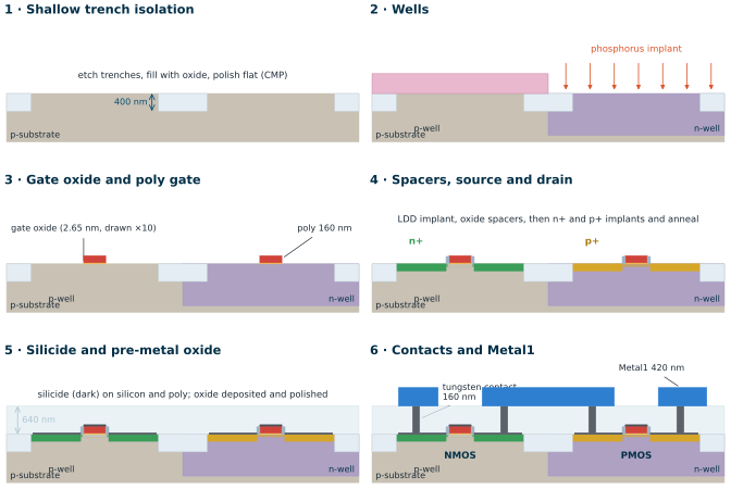
- Shallow trench isolation (STI). Trenches 400 nm deep are etched around every active area, filled with oxide and polished flat. Wherever you did not draw Activ (SG13G2) or diff/tap (SKY130), there will be trench oxide. The oxide squeezes the silicon next to it, which is why a transistor’s current depends on how far its gate sits from the trench edge, the length-of-diffusion effect of Chapter 15.
- Wells. Masked implants form the n-wells for PMOS devices and the p-wells for NMOS devices. Dopant ions scatter off the edge of the resist mask, so a transistor close to a well edge gets a slightly different threshold: the well-proximity effect.
- Gate oxide and poly gate. A gate oxide a few nanometres thick is grown (2.65 nm for the SG13G2 core NMOS, 4.15 nm in the SKY130 1.8 V model, Chapter 3), a thick-oxide region is added for the higher-voltage devices, and the polysilicon (160 nm in SG13G2, 180 nm in SKY130) is deposited and etched into gates. The poly etch is the most critical lithography step of the process, because it sets the channel length.
- Spacers, source and drain. A light implant (the lightly doped drain, LDD) is followed by oxide spacers on both sides of each gate and then the heavy n+ and p+ implants, which therefore stay a spacer width away from the channel. Angled halo implants under the gate edges, which give the SG13G2 core devices their strong length dependence (Chapter 6), are done at this stage. An anneal activates everything.
- Silicide and pre-metal oxide. A metal is deposited and reacted with the exposed silicon and poly to form a low-resistance silicide; where a SalBlock (SG13G2) or poly-resistor implant layer (SKY130) blocks it, the poly keeps its high sheet resistance, which is how the precision resistors of Chapter 3 are made. A thick oxide (640 nm up to Metal1 in SG13G2) covers everything and is polished flat.
- Contacts and the first metal. Contact holes are etched down to silicide, filled with tungsten and polished, and the first metal is patterned on top. SKY130 inserts its local interconnect here: the contacts (licon) end on the 100 nm li1 layer, 0.61 µm above the silicon, and a second contact (mcon) reaches met1, whose bottom is 1.05 µm above the silicon [20].
The front end has density rules of its own. CMP polishes dense and sparse regions at different rates, so the foundry asks for a minimum and maximum fraction of the chip covered by each layer. In SG13G2, Activ must cover 35–55 % of the chip and 25–65 % of every 800 µm × 800 µm window, and GatPoly at least 15 % [16]; the open_pdks density script for SKY130 asks for 33–57 % diffusion in every 700 µm × 700 µm window [20]. A small analog block never meets these numbers on its own: they are met with fill, dummy shapes added in the empty space (Section 17.6).
SG13G2 vs SKY130 · The same front end, different numbers
The two front ends follow the same recipe: STI, wells, one thin and one thick gate oxide, poly gates, spacers, silicide and tungsten contacts. The differences you feel as a designer come from the numbers: SG13G2’s thinner oxide (2.65 nm against 4.15 nm) gives more current per volt but less intrinsic gain, and its contacts land directly on Metal1, while SKY130’s land on the resistive li1 layer. SG13G2 also adds the steps that build its SiGe HBT (a buried n+ layer and an epitaxial SiGe base), which a CMOS-only designer never sees.
17.3 The back end of line
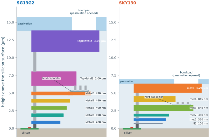
Above the first metal the process repeats one cycle per layer: deposit oxide, polish it, etch via holes, fill them with tungsten, deposit metal, pattern it by lithography and etch. Both of our processes use aluminium wiring patterned by etching [15, 18], rather than the copper inlaid into etched trenches (damascene) of finer nodes. The MIM capacitor needs one extra mask for its top plate and a very thin dielectric; the last steps deposit the passivation, a hard layer of oxide and nitride that seals the chip against moisture and scratches, and open it over the bond pads.
Figure 17.2 shows the finished back end of both processes on the same vertical scale.
Density, fill and slots
CMP of the inter-metal oxide has the same problem as in the front end: a large empty area polishes deeper than a dense one, and a wide metal plate dishes in the middle. The result is a wafer whose layer thicknesses, and so wire resistances and capacitances, depend on the local pattern. The foundries therefore set density windows for every metal (Table 17.1).
Table 17.1. Metal density rules [16, 20]. SKY130 values are those checked by the open_pdks density script.
| Quantity | SG13G2 | SKY130 |
|---|---|---|
| Thin metals, whole chip | 35–60 % (M1.j/k, Mn.j/k) | — |
| Thin metals, local window | 25–75 % in every 800 × 800 µm² (MFil.h/k) | 35–60 % (li1, met1–met4) in every 700 × 700 µm², 70 µm steps |
| Top metals | 25–70 % (TM1.c/d, TM2.c/d) | met5: 45–76 % |
| Wide metal | slits needed above 30 µm width (Slt.c) | — |
| Fill tools | KLayout macros sg13g2_filler_*.lym |
Magic generate_fill.py, check_density.py |
Density is not only a manufacturing nicety. The SG13G2 rules warn that minimum-width lines in a region with less than 30 % metal coverage come out with 10 % more sheet resistance [16], because the thinner metal left after polishing a sparse region conducts less. Fill also adds capacitance: a floating fill square between a signal wire and ground couples the two, and fill under a sensitive node such as the gate of an input transistor or the plates of a matching capacitor array changes their capacitance by an amount your pre-fill extraction never saw. Both PDKs let you exclude fill locally (Metal(n):nofill and NoMetFiller in SG13G2), as long as the window rules are still met; Chapter 16 shows how to extract the block after fill.
The antenna effect
While a metal layer is being etched in a plasma, every wire that is not yet connected to a diffusion collects charge, like an antenna, and discharges it through the only path it has: the gate oxide of the transistors it is connected to. If the wire is large compared with the gate, the current can damage the oxide or shift the threshold voltage. The rule therefore limits the ratio of the antenna area to the gate area it is connected to:
\[\mathrm{AR} = \frac{A_\mathrm{metal}}{A_\mathrm{gate}} \leq \mathrm{AR}_\mathrm{max}. \tag{17.1}\]The details differ between the PDKs (Table 17.2). SG13G2 counts the drawn top area of all metal levels connected to the gate, cumulatively up to TopMetal2 [16]. The SKY130 rules in Magic use the sidewall area of each wire (its perimeter times its thickness), level by level [20].
Table 17.2. Main antenna limits [16, 20].
| Quantity | SG13G2 | SKY130 |
|---|---|---|
| Poly | 200 (GatPoly over field / gate, Ant.a) | 50 (sidewall) |
| Metal, no protection diode | 200 (cumulative M1–TM2 area, Ant.b) | 400 per level (sidewall, met1–met5) |
| Metal, with protection diode | 20 000 (Ant.e) | 2200 + 400 × diode area |
| Checked by default? | no: run_drc.py --antenna |
Magic check_antenna.py |
Worked example 17.1 · An antenna violation in a bias line
A bias line in SG13G2 runs 200 µm in Metal2 (0.2 µm wide) and 20 µm in Metal1 (0.16 µm wide) to the gate of a small current-mirror device of W = 0.5 µm and L = 0.5 µm. The cumulative metal area is \(200 \times 0.2 + 20 \times 0.16 = 43.2\ \mu\mathrm{m^2}\) and the gate area \(0.25\ \mu\mathrm{m^2}\), so by Eq. (17.1) AR = 173: just under the limit of 200. Route the same line in Metal3 instead and it is still 173, because SG13G2 counts all levels together; make it 300 µm long and AR = 253, a violation.
The fixes, in order of preference: connect the gate to a drain or a small reverse-biased diode on Metal1 (the limit rises to 20 000), or break the long line and jump up to a higher metal close to the gate, so that the long run is connected to the gate only in the last etch step. The IHP rules recommend the diode for every gate in circuits that are sensitive to threshold shifts, such as matched analog pairs [16]. A gate of the course OTA’s input pair (W = 18.2 µm, L = 3 µm, 54.6 µm²) could tolerate 10 900 µm² of metal: large analog devices rarely violate, minimum-size ones often do.
17.4 Packaging and bonding
A finished die is a few square millimetres of glass-covered silicon. To use it, the foundry or a packaging house saws the wafer along scribe lines between the dies, glues each die onto a lead frame or board, connects its pads to the package leads with thin wires, and seals it. Figure 17.3 shows the parts involved.
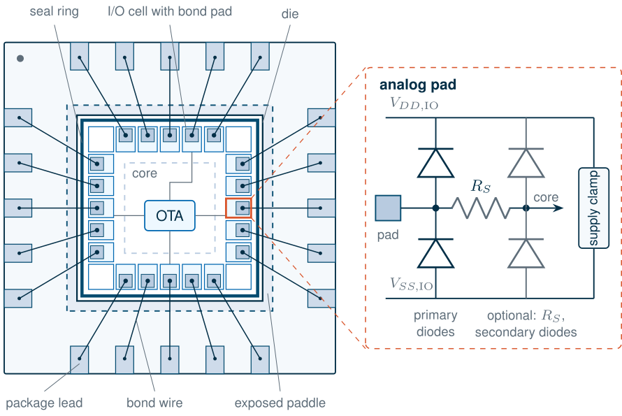
The seal ring. Around the edge of every die runs an unbroken wall of every metal and via layer, from the substrate to the top metal, enclosed by passivation. It stops cracks from the saw and moisture from creeping in sideways. SG13G2 has its own rules for it (an EdgeSeal ring of every layer, at least 3.5 µm wide, one per chip, enclosed by an unbroken passivation ring) and a seal-ring PCell in its KLayout library [16, 14]; open_pdks ships a seal-ring generator for SKY130 [20]. On Tiny Tapeout and on ChipFoundry’s harness the seal ring and the pad ring are part of the chip you are placed in.
Bond pads. A pad is a square of top metal, typically 60 to 100 µm on a side, under an opening in the passivation. The SG13G2 rules recommend pads at least 30 µm wide (at most 150 µm), no devices under the pad because bonding stresses the silicon, and 25 µm between pad opening and seal ring for wedge bonding [16].
ESD protection. A person who touches a pin can discharge a few kilovolts through it; a gate oxide of a few nanometres breaks down at a few volts. Every pad therefore has an electrostatic-discharge (ESD) path that conducts the discharge current to a supply rail before it reaches a gate [60]: a diode from the pad to each rail, and a large supply clamp transistor between the rails that turns on during the fast edge of the discharge. Table 17.3 lists what the two PDKs provide.
Table 17.3. I/O and ESD cells for analog signals, from the PDKs' cell libraries and SPICE netlists in IIC-OSIC-TOOLS 2026.10 [14, 20].
| Quantity | SG13G2 | SKY130 |
|---|---|---|
| I/O library | sg13g2_io: 80 × 180 µm cells, 180 × 180 µm corner |
sky130_fd_io (SkyWater) and sky130_ef_io (Efabless wrappers) |
| Analog pad | sg13g2_IOPadAnalog |
sky130_ef_io__analog_pad (no ESD), __analog_esd_pad, __analog_minesd_pad |
| Primary protection | two dantenna diodes to iovss and two dpantenna diodes to iovdd (27.8 × 1.26 µm each), plus 3.3 V MOS clamps |
5 + 5 diodes (esd_pad) or 1 + 1 (minesd_pad) to VSSIO and VDDIO |
| Secondary protection | 587 Ω rppd series resistor and small diodes to a second core-side pin, padres |
none |
| Supply pads | IOPadVdd, IOPadVss (core), IOPadIOVdd, IOPadIOVss (3.3 V I/O) |
supply pads with clamps in sky130_fd_io |
The protection is not free for an analog signal. Each diode is a junction capacitance on your node, the diodes leak and that leakage doubles about every 10 °C, and the 587 Ω secondary resistor of the SG13G2 analog pad adds thermal noise (\(\sqrt{4kTR} = 3.1\ \mathrm{nV}/\sqrt{\mathrm{Hz}}\) at 27 °C) and a pole with whatever capacitance sits behind it. That is why the SG13G2 cell offers both the direct pad node and the protected padres node, and why the SKY130 library includes an analog pad with no protection at all, to be used only when the circuit behind it protects itself.
Packages
The package fixes how many pins you have and how much inductance and capacitance sit in series with each. Three choices cover almost every student chip:
- QFN (quad flat no-lead): a square plastic package with pads on the underside and a large exposed paddle in the middle that is soldered to the board’s ground. Its leads are short, so it adds little inductance. IHP offers QFN packaging for its open runs, from QFN24 (4 × 4 mm, dies up to 2 × 2 mm) to QFN64 (9 × 9 mm), at €690 for ten QFN24 parts plus €320 per bonding diagram [25]. ChipFoundry’s chipIgnite delivers 100 QFN parts [28].
- DIP (dual in-line) and other through-hole packages: easy to put in a socket on a breadboard, but their long leads add several nanohenries per pin. Fine for DC and audio-frequency tests, poor for a 20 MHz amplifier.
- Chip-on-board (COB): the bare die is glued directly onto the test board and bonded to its traces, then covered with a drop of epoxy. It gives the shortest connections of all and needs no package; Tiny Tapeout’s TT08 chips, for example, arrived this way [31].
Bond wires and supply bounce
A bond wire is a gold or aluminium wire, typically 25 µm in diameter and 1 to 3 mm long. At the frequencies of interest its resistance is small but its inductance is not. Grover’s formula for a straight round wire of length \(l\) and radius \(r\) carrying a uniform current is [64]
\[L_w = \frac{\mu_0 l}{2\pi}\left[\ln\!\left(\frac{2l}{r}\right) - \frac{3}{4}\right]. \tag{17.2}\]For a 25 µm wire it gives 0.36 nH at 0.5 mm, 0.87 nH at 1 mm, 2.0 nH at 2 mm and 3.3 nH at 3 mm: the familiar rule of thumb of about 1 nH per millimetre. A 2 mm gold wire has only 0.1 Ω of DC resistance. The package lead and the board trace add their own inductance in series.
The supply current of a chip reaches the circuit through the VDD wire and returns through the VSS wire, so the loop inductance is the sum of both, \(L = L_\mathrm{VDD} + L_\mathrm{VSS}\) (less if the two wires run close together, because their mutual inductance subtracts). When the current drawn by the chip changes by \(\Delta I\) in a time \(t_r\), the on-chip supply drops by
\[\Delta V \approx L\,\frac{\Delta I}{t_r} \tag{17.3}\]during the edge. The cure is an on-chip decoupling capacitor \(C\) between VDD and VSS, which supplies the fast current locally. But \(L\) and \(C\) form a resonant circuit. Its natural frequency and characteristic impedance are
\[f_0 = \frac{1}{2\pi\sqrt{LC}}, \qquad Z_0 = \sqrt{\frac{L}{C}}, \qquad \Delta V_\mathrm{peak} \approx \Delta I\, Z_0\,\frac{\sin x}{x}, \tag{17.4}\]where \(x = \omega_0 t_r/2 = \pi f_0 t_r\) and the factor \(\sin x / x\) accounts for the finite rise time of the current step (it is 1 for an instant step). The ringing decays with a time constant \(2L/R\), where \(R\) is the loop resistance, so its quality factor is \(Q = Z_0/R\).
Derivation · Peak droop of an LC supply for a ramped current step
Model the supply as an ideal source behind a series inductance \(L\) (resistance neglected), the decoupling capacitor \(C\) on the chip, and a current sink that steps by \(\Delta I\). For an instant step the capacitor must deliver the whole \(\Delta I\) at first, and the node voltage responds as \(\Delta V(t) = -\Delta I\, Z_0 \sin(\omega_0 t)\) with \(\omega_0 = 1/\sqrt{LC}\) and \(Z_0 = \sqrt{L/C}\): the energy balance \(\tfrac{1}{2}L\Delta I^2 = \tfrac{1}{2}C\Delta V^2\) gives the same amplitude. A linear ramp of duration \(t_r\) is a sum of small steps \(\Delta I\,\mathrm{d}\tau/t_r\) spread over \(0 \le \tau \le t_r\). After the ramp their responses add up to
\[\Delta V(t) = -\frac{\Delta I\,Z_0}{t_r}\int_0^{t_r}\!\sin\omega_0(t-\tau)\,\mathrm{d}\tau = -\frac{\Delta I\,Z_0}{\omega_0 t_r}\Big[\cos\omega_0(t-t_r) - \cos\omega_0 t\Big],\]and the bracket is \(2\sin(\omega_0 t_r/2)\,\sin\omega_0(t - t_r/2)\): an oscillation of amplitude
\[\Delta I\, Z_0\,\frac{2\sin(\omega_0 t_r/2)}{\omega_0 t_r} = \Delta I\, Z_0\,\frac{\sin x}{x}, \qquad x = \frac{\omega_0 t_r}{2}.\]For \(t_r \ll 1/f_0\) the factor tends to 1; it falls as the edge becomes slow compared with the resonance.
The derivation contains a useful rule: a decoupling capacitor only helps if \(Z_0\Delta I < L\Delta I/t_r\), that is if \(C > t_r^2/L\). A smaller capacitor just moves the resonance close to the edge rate and rings.
Worked example 17.2 · Supply bounce on the course-project OTA
The OTA of Chapter 12 shares its supply pads with a block that switches \(\Delta I\) = 5 mA with 0.5 ns edges (a small digital block or an output driver). Each supply has one 2 mm bond wire: \(L\) = 2 × 2.0 = 4.0 nH, \(R\) = 0.2 Ω.
No decoupling. Eq. (17.3): \(\Delta V = 4\ \mathrm{nH} \times 5\ \mathrm{mA}/0.5\ \mathrm{ns} = 40\) mV. To do better, Eq. (17.4) needs \(C > t_r^2/L = 62.5\) pF.
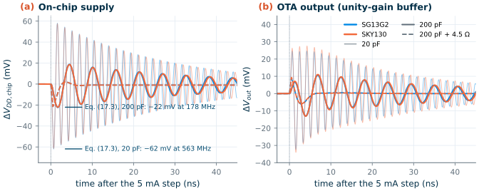
20 pF of MIM decoupling. \(Z_0\) = 14.1 Ω, \(f_0\) = 563 MHz, \(x\) = 0.88 and \(\sin x/x\) = 0.87, so \(\Delta V_\mathrm{peak}\) = 5 mA × 14.1 Ω × 0.87 = 62 mV, worse than no capacitor at all, and ringing with \(Q\) = 71.
200 pF. \(Z_0\) = 4.47 Ω, \(f_0\) = 178 MHz, \(\sin x/x\) = 0.99: \(\Delta V_\mathrm{peak}\) = 22 mV, decaying with \(2L/R\) = 40 ns (\(Q\) = 22).
200 pF with 4.5 Ω in series (\(\approx Z_0\)) damps the resonance: the first droop stays near \(\Delta I Z_0\), but the ringing dies within one cycle.
Figure 17.4 shows the simulation of all cases with the OTA connected as a unity-gain buffer, with real MIM capacitors from each PDK. The simulated peaks are 62.0 and 61.5 mV for 20 pF (SG13G2, SKY130), 22.3 and 22.1 mV for 200 pF, and 58 and 64 mV with no decoupling; the ringing frequencies are 564/561 MHz and 178/176 MHz. With decoupling, hand analysis and simulation agree to 1 %; without it, the 0.1 pF or so left on the supply rings at 7 to 10 GHz and the droop overshoots the 40 mV of Eq. (17.3). The OTA cannot reject this: at 178 MHz, far above its 21 MHz unity-gain frequency, its output moves by 13.0 mV (SG13G2) and 13.1 mV (SKY130) for a 22 mV supply droop, and the damped capacitor reduces that to 8.7 and 9.4 mV.
What this means for your design
- Give a sensitive block its own supply pads, so that no switching current flows through its bond wires, and place VDD and VSS pads next to each other so that their mutual inductance reduces the loop.
- Size the on-chip decoupling from \(C > t_r^2/L\), not from a habit. 200 pF of MIM capacitance is large: 132 500 µm² in SG13G2 and 100 000 µm² in SKY130, more than the OTA itself. A thin-oxide MOS capacitor is far denser: our simulations give 12.7 fF/µm² for an SG13G2 core NMOS and 7.9 fF/µm² in SKY130, against 1.5 and 2.0 fF/µm² for the MIM capacitors. It leaks (0.42 nA/µm² of gate current in the SG13G2 model at 1.2 V, none in the SKY130 model), and its channel resistance provides the damping of Figure 17.4 for free.
- Keep the package inductance low: short bond wires, several wires in parallel for supplies, QFN or chip-on-board rather than DIP for anything above audio frequencies.
17.5 Multi-project wafers and open shuttles
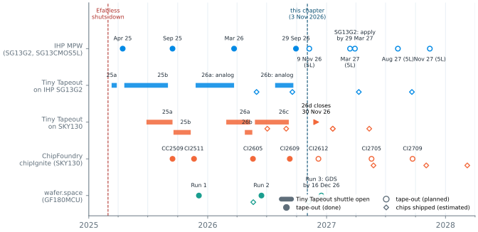
A full mask set for a 130 nm process costs far more than a student project can pay. A multi-project wafer (MPW), or shuttle, shares one mask set and one wafer lot among many designs: each customer pays for the area of their die, receives a few dozen dies, and the foundry or a broker collects the designs before a fixed tape-out date. Tiny Tapeout goes one level further: it shares a single die among hundreds of small designs, each occupying one or a few tiles behind an on-chip multiplexer, and sells each tile for a small fee [12]. Chapter 1 told the history up to 2026; here is where things stand as of November 2026.
SG13G2: IHP’s Open-Silicon MPW
IHP ran free open-source shuttles for non-commercial designs from 2023 to 2025 (Chapter 1). In 2026 they were replaced by a low-cost, paid Open-Silicon MPW programme [25]:
- The design must be released under the Apache 2.0 licence, prepared with open-source EDA tools and published in IHP’s GitHub repository [48]; participants sign a participation agreement. Designs that must stay private get 20 % off the normal MPW price instead.
- SG13G2 costs €2 800 per mm²; the CMOS-only five-metal SG13CMOS5L costs €1 500 per mm² (€1 227 on the 9 November 2026 run). A run starts only once enough area has been booked, and the price per mm² falls as the total grows.
- Each standard submission returns 40 bare dies; QFN packaging is extra (Section 17.4). Processing takes about six months for SG13G2.
- The schedule lists an SG13G2 run on 29 September 2026 (registration closed 21 September), SG13CMOS5L runs on 9 November 2026, 14 March, 8 August and 14 November 2027, and an SG13G2 run in 2027 with registration by 29 March 2027.
Tiny Tapeout, on both PDKs
Tiny Tapeout now runs shuttles on IHP SG13G2, on SKY130 (through ChipFoundry) and on GF180MCU (through wafer.space) [12]. Analog designs were first accepted on TT06 in 2024 on SKY130 [11]; on IHP, analog designs arrived with TTIHP26a (closed 23 March 2026), and TTIHP26b (closed 21 September 2026, 123 designs) carried bandgap references and LDO regulators among its analog projects, with chips expected in June 2027 [12, 32]. On 3 November 2026 two shuttles were open: TTSKY26d, closing on 30 November 2026, and TTGF26c, closing on 7 December 2026; no IHP shuttle was open [33].
An analog Tiny Tapeout design lives in a tile of fixed size and connects to the outside through a limited number of analog pins. For SKY130 the specification gives tiles of about 160 × 225 µm (1 × 2 tiles) or 334 × 225 µm (2 × 2), up to six analog pins ua[0] to ua[5], each with less than 500 Ω and less than 5 pF between the pad and your pin and at most 4 mA, met5 reserved for the power grid, and a 1.8 V supply plus an optional 3.3 V one; analog projects cost at least €140 (two tiles at €70) plus €40 for each of the first two analog pins and €100 for each further one [47]. Templates for SG13G2 analog tiles exist in the same two sizes; check the current prices and pin limits for your shuttle in the Tiny Tapeout calculator before you design.
Common pitfall · Designing for a load you will never have
A Tiny Tapeout analog pin puts up to 500 Ω and 5 pF, then a bond, a board trace and your probe, between your output and the instrument. The course OTA was compensated for a 2 pF load; Section 17.7 shows that 12 pF more drops its phase margin from 67° to about 35°. Decide early what the pin will drive and either design for that load or add an on-chip buffer.
SKY130 after Efabless
Efabless, which ran Google’s free SKY130 shuttles and Tiny Tapeout’s first runs, shut down at the start of March 2025 [24]. Tiny Tapeout’s TT10 was cancelled and TT09, which had already closed with 369 designs, still has no delivery date [12]. In September 2025 Umbralogic Technologies, trading as ChipFoundry, bought Efabless’s intellectual property and technology assets [27], and it now runs the SKY130 shuttles: its chipIgnite service costs $14 950 per tape-out for up to 15 mm² of user area inside a standard harness with 38 configurable I/Os (digital or analog), and returns 100 QFN parts or bare dies with an evaluation board [28]. Its next shuttles are CI2612 (commitment 4 November 2026, tape-out 7 December 2026, delivery 25 May 2027), CI2705 (tape-out 19 May 2027) and CI2709 (22 September 2027). Tiny Tapeout’s SKY130 shuttles ride on these runs [30, 12].
Other routes
For completeness: wafer.space offers GF180MCU (a 180 nm open PDK) runs with 1 000 dies per slot, from $3 000 for a 1.94 × 2.53 mm quarter slot to $8 000 for a 3.93 × 5.12 mm slot at standard prices; Run 3 takes GDS files until 16 December 2026 and ships in the second quarter of 2027 [29]. It does not use either of this book’s PDKs.
Table 17.4. Routes to silicon, as of 3 November 2026 [25, 47, 28, 29]. Prices exclude tax, shipping and boards; check the providers before you plan.
| Route | PDK | Area you get | Price | Parts returned | Next deadline |
|---|---|---|---|---|---|
| IHP Open-Silicon MPW | SG13G2 | your own die, any size | €2 800/mm² | 40 bare dies | registration by 29 Mar 2027 |
| IHP Open-Silicon MPW | SG13CMOS5L | your own die | €1 227–1 500/mm² | 40 bare dies | 1 Mar 2027 (run of 14 Mar) |
| Tiny Tapeout analog | SKY130 (SG13G2 on IHP shuttles) | 0.036 or 0.075 mm² tile | from €140 + analog pins | chip on a demo board (bought separately) | TTSKY26d: 30 Nov 2026 |
| ChipFoundry chipIgnite | SKY130 | up to 15 mm² | $14 950 | 100 QFN parts | CI2612: commit 4 Nov 2026 |
| wafer.space | GF180MCU | 4.9–20.1 mm² die | $3 000–8 000 | 1 000 dies | Run 3: 16 Dec 2026 |
17.6 Preparing a submission
Every foundry and every shuttle has its own submission checklist, but they all check the same things, in roughly the order of Figure 17.6.
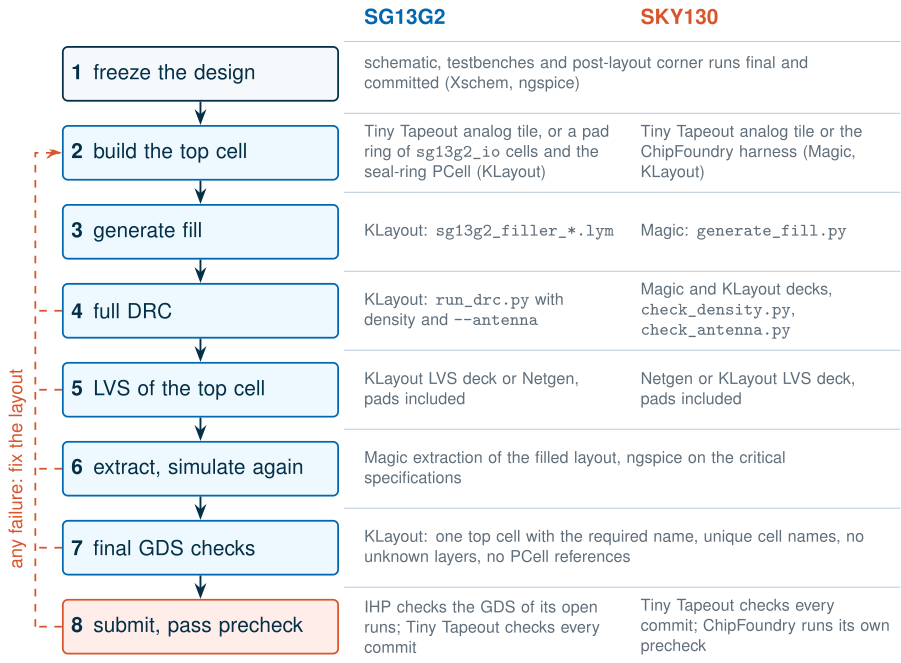
- Freeze the design. The schematic, the testbenches and the post-layout simulation over corners (Chapter 16) are final and committed.
- Build the top cell. Place the block in the template of your route: a Tiny Tapeout analog tile with its power stripes and pins on met4, the ChipFoundry harness, or for an IHP die your own pad ring of
sg13g2_iocells and a seal ring. Connect every pad you use and tie every unused input. - Fill. Generate the fill shapes for active, poly and every metal (
sg13g2_filler_*.lymin KLayout for SG13G2,generate_fill.pyin Magic for SKY130), with exclusion layers over your sensitive devices. - Full DRC. Run the complete deck, not the quick one: for SG13G2
run_drc.pywith density and--antennaenabled (antenna rules are off by default), for SKY130 the full Magic and KLayout decks pluscheck_density.pyandcheck_antenna.py. Zero violations, or a written waiver from the provider. - LVS of the top cell, including the pads, against a top-level netlist.
- Extract and simulate again with fill in place, at least the critical specifications.
- Final GDS checks. One top cell with the required name, no empty or unknown layers, no PCells left as references to scripts, all cells uniquely named so that they do not clash with other designs on the shuttle.
- Submit, then pass the provider’s own precheck (Tiny Tapeout runs one on every commit of your repository; IHP checks the GDS of its open runs before accepting it) and publish the design if the route requires it.
Try it · Lab 8
Lab 8 ends with a clean DRC and LVS of your OTA. Take it one step further: place the layout in a Tiny Tapeout analog template for your PDK, generate fill, and run the full DRC with density and antenna checks enabled. Note how many violations appear that the block-level DRC never reported.
17.7 Testing your silicon
Months after tape-out, the dies or packaged parts arrive. Plan the measurement before tape-out, because what you can measure depends on what you put on the chip and on the board.
The test board
Figure 17.7 shows a test setup for the course-project OTA. Its essentials are the same for any analog chip:
- Clean supplies. A low-noise regulator for the analog supply, separate from any digital supply; decoupling capacitors (100 nF plus 1–10 µF) as close to each supply pin as possible; a solid ground plane under the chip, with the QFN paddle soldered to it.
- A bias current, here the OTA’s 10 µA reference, from a precision resistor to a known voltage or a source-measure unit, so that you can measure and vary it.
- Input and output paths with known impedances. Short traces, a footprint for a series resistor at every pin (0 Ω to begin with), and test points.
- Buffering. The OTA was designed for a 2 pF load. It cannot drive a coaxial cable or a 10 pF oscilloscope probe without losing its phase margin (Figure 17.8), so either measure through a low-capacitance active probe, or add a buffer: an on-chip source follower or test buffer (designed and simulated with the chip), or a fast FET-input op amp next to the chip on the board.
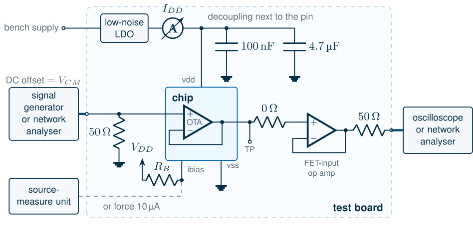
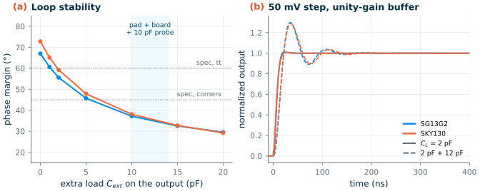
Figure 17.8 quantifies the problem. The phase margin of the OTA falls from 67.0° (SG13G2) and 72.8° (SKY130) at its 2 pF design load to 60.6° and 65.2° with only 1 pF more, below the 45° corner specification beyond about 5 pF, and to 37.2° and 38.1° with 10 pF extra. With 12 pF extra, a pad, a short trace and a passive probe, a 50 mV step overshoots by 29.9 % and 28.8 % instead of 1.2 % and 0.7 %. A measurement like that would tell you about your test fixture, not about your amplifier. The cause is the output pole \(g_{m6}/C_L\) of Chapter 12, which moves down towards the unity-gain frequency as the load grows.
What to measure, and how
Table 17.5. A measurement plan for the course-project OTA. Expected values are the Chapter 12 simulations at tt, 27 °C, with the range over process corners and −40 to 125 °C in brackets.
| Measurement | Method and equipment | SG13G2 expected | SKY130 expected |
|---|---|---|---|
| Supply current | source-measure unit or ammeter, OTA biased, no signal | 93 µA (112 µW at 1.2 V) | 90 µA (162 µW at 1.8 V) |
| Input offset | unity-gain buffer, DC voltmeter, many dies | a few mV, statistical (Chapter 13) | same |
| Unity-gain frequency, phase margin | small-signal step or frequency response with a network analyser, known load | 21.5 MHz (15.9–27.4), 67° | 21.7 MHz (17.2–26.2), 73° |
| Slew rate | large step, oscilloscope behind a buffer | 15.6 V/µs | 14.6 V/µs |
| DC gain | nulling loop or closed loop with a large resistor ratio | 62.2 dB (60.9–63.1) | 75.7 dB (73.1–76.6) |
| PSRR, CMRR | small signal on the supply or on both inputs | 67.8 dB, 65.8 dB at DC | 77.0 dB, 72.0 dB at DC |
| Noise | low-noise preamplifier and spectrum analyser, batteries or a quiet supply | input-referred spectrum of Chapter 13 | same |
Compare like with like. Before you compare a measurement with a simulation, put the test fixture into the simulation: the pad and ESD capacitance, the bond-wire and board inductance, the probe or buffer, the real bias current. Then compare measured values with the range over corners and temperature, not with the typical number, and measure several dies, because a single die is one sample of the process and mismatch distributions. A measurement inside the simulated range confirms the design; a measurement outside it, on several dies and in the same direction, points to a modelling or layout effect that is worth a paper.
- A wafer is built from repeated lithography, etch, implant, deposition, anneal and polish steps: the front end makes the transistors (STI, wells, gate oxide and poly, spacers and source/drain, silicide, contacts) and the back end the wiring. Most design rules are the limits of one of these steps.
- At tape-out the foundry needs a GDS that passes the full deck: fill for every layer (SG13G2 metals 35–60 % globally, SKY130 35–60 % per 700 µm window), antenna rules (checked separately in SG13G2), a seal ring and pads, and a clean top-level LVS.
- Pads bring ESD protection (diodes to both rails and clamps; a 587 Ω secondary resistor in the SG13G2 analog pad), capacitance, leakage and bond-wire inductance of about 1 nH per millimetre.
- A current step \(\Delta I\) through a bond-wire loop \(L\) with on-chip decoupling \(C\) produces a droop of about \(\Delta I\sqrt{L/C}\) that rings at \(1/(2\pi\sqrt{LC})\); decoupling only helps if \(C > t_r^2/L\). In the worked example, 5 mA through 4 nH gave 62 mV with 20 pF and 22 mV with 200 pF, within 1 % of simulation, and the OTA passed most of it to its output.
- As of November 2026, SG13G2 designs reach silicon through IHP’s paid Open-Silicon MPW (€2 800/mm², open-source designs) and Tiny Tapeout’s IHP shuttles; SKY130 designs through ChipFoundry and Tiny Tapeout’s SKY130 shuttles.
- Plan the measurement before tape-out: a 12 pF fixture drops the OTA’s phase margin to about 35°, so buffer the output or design for the real load, and compare measurements with simulated corner ranges that include the fixture.
Further reading
- J. D. Plummer, M. D. Deal and P. B. Griffin [63]: the process steps of Sections 17.2 and 17.3 in depth, with the physics of each.
- A. Hastings, The Art of Analog Layout [60]: pads, ESD structures and assembling a die from a layout designer’s point of view.
- The IHP SG13G2 layout rules [16]: the fill, density, seal-ring, pad and antenna rules quoted in this chapter, with figures.
- Tiny Tapeout’s analog specification [47] and IHP’s Open-Silicon MPW page [25]: read the current versions before you start a design for either route.