Chapter 29
Power Devices, Guard Rings and ESD
Large transistors carry amperes through narrow metal, injected carriers wander far through the substrate, and a touch of a finger delivers kilovolts. All three are layout problems. This chapter draws large transistors with the PDKs' generators, solves the resistive network of their metal to see where the current goes, follows injected electrons to the guard rings that should catch them, and sends a simulated human-body discharge into the ESD protection that each PDK actually ships.
- Lay out large transistors as multi-finger arrays and waffles, and know what sets their pitch in each PDK.
- Calculate the on-resistance of a large transistor from its model and its metallization, by hand and with a network model, and choose a metallization pattern.
- Estimate how much of an injected minority-carrier current reaches a victim, and what a guard ring buys.
- Explain the HBM and CDM events and the requirements an ESD network must meet.
- Use the ESD diodes, clamps and pad cells of SG13G2 and SKY130, simulate a discharge through them, and lay out the ESD current path.
Contents
Chapter 24 set the current-density limits of every metal and showed how guard rings stop latch-up; Chapter 17 introduced the pad ring and listed the I/O cells of both PDKs. This chapter goes into the devices that carry large currents on purpose (power transistors), the carriers they inject by accident, and the protection against the largest current a chip ever sees, an electrostatic discharge. The layouts come from IHP’s KLayout PyCells and Magic’s SKY130 generator, the device behaviour from each PDK’s models in IIC-OSIC-TOOLS, and the ESD networks from the PDKs’ own I/O libraries [35, 14, 20]:
python3 tools/layout/ch29/power_layouts.py      # generators, buses, waffles, IO cells, 3D model
python3 tools/layout/ch29/power_layouts.py drc  # KLayout DRC of the power transistors and waffles
python3 tools/figs/_ch29_sim.py                 # on-resistance, HBM and TLP-like runs, both PDKs (about five minutes)
python3 tools/figs/ch29_power.py                # metal network and injection models, figures, ch29_numbers.json
29.1 Large transistors: fingers, waffles and metallization
Many small transistors in parallel
A switch of 1 Ω, an output stage that sinks 50 mA, or the clamp of an ESD network needs a transistor that is hundreds or thousands of micrometres wide. Nobody draws it as one long gate. It is folded into \(N\) gate fingers of width \(W_f\) that share their source and drain diffusions with their neighbours, exactly as Chapter 15 folded the OTA’s devices, only many more of them. In the linear region the channel behaves as a resistor whose value scales inversely with the total width \(W = NW_f\):
Key equation · On-resistance of a large MOSFET
\[R_{on} = \frac{R_{on}W}{W} + R_{contacts} + R_{metal}, \qquad R_{on}W \approx \frac{L}{\mu C_{ox}(V_{GS} - V_{TH})}. \tag{29.1}\]\(R_{on}W\) (Ω·µm) is a property of the device type at a given \(V_{GS}\) and temperature; it comes from the PDK model. The other two terms come from the layout.
The square-law expression only explains the trends: \(R_{on}W\) is proportional to the gate length and falls as the gate overdrive rises. The numbers must come from the models. Figure 29.2 gives them for the core and thick-oxide transistors of both PDKs, and Section 29.2 uses them.
What the generators draw
Figure 29.1 shows a 16-finger NMOS in each PDK as the generators draw it, with the metal buses our script adds on top. IHP’s sg13_lv_nmos PyCell (W = 80 µm, ng = 16, L = 0.13 µm) places the source and drain diffusions at a pitch of 0.51 µm with a first-metal stripe on each, and leaves the gates unconnected; Magic’s nfet_01v8 (16 fingers of 5 µm, L = 0.15 µm) uses a pitch of 0.48 µm and adds its own gate strap and guard ring [14, 20]. power_layouts.py then widens each first-metal finger enough to land a via (0.29 µm in SG13G2, 0.26 µm in SKY130), drops vias only where a finger passes under its own bus, and draws two second-metal buses over the device: the drain bus over the upper half of the fingers, the source bus over the lower half. In SG13G2 it also adds a poly gate strap and a p+ guard ring. Both layouts pass their KLayout rule decks with zero violations.
The pitch of such an array has three limits [61]. The front end needs a gate, a contact and two contact-to-gate spacings: \(0.13 + 0.16 + 2 \times 0.11 = 0.51\) µm in SG13G2 (Chapter 23). The first metal needs its finger width plus one spacing: \(0.29 + 0.18 = 0.47\) µm with a via landing. The via layer needs the via, its enclosure and the metal spacing again. In SG13G2 the front end sets the pitch; Magic’s SKY130 generator draws 0.48 µm, wider than the 0.43 µm minimum of \(0.15 + 0.17 + 2 \times 0.055\), and the first metal (0.26 + 0.14 = 0.40 µm) fits inside it too. A power transistor in either PDK therefore costs no area for its metal, as long as each finger carries one via column.
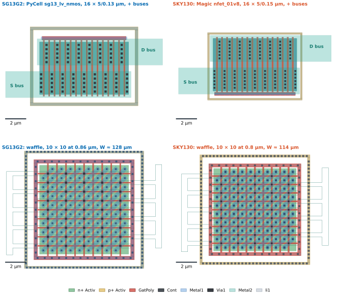
sg13_lv_nmos and Magic's nfet_01v8, 16 × 5 µm, with second-metal buses over the device (drain over the upper half, source over the lower half). Bottom: waffle NMOS drawn with klayout.db from the rule tables, 10 × 10 openings; the 45° first-metal stripes run under the second-metal combs. The SG13G2 waffle has one violation, Gat.f, which forbids bent gates on active; the other three layouts are clean. Generated by tools/layout/ch29/power_layouts.py.The waffle
A waffle transistor replaces the parallel gate fingers with a grid of poly. Every square opening of the grid is a source or a drain, arranged like a chessboard, so every opening is surrounded by gate on four sides instead of two. With openings of side \(a\) and a gate length \(L\), the cell pitch is \(p = a + L\); each opening contributes four gate edges of length \(a\), and each edge is shared by two openings. The gate width per unit area is therefore
\[\frac{W}{A}\bigg\vert_{waffle} = \frac{2a}{(a+L)^2}, \qquad \frac{W}{A}\bigg\vert_{fingers} = \frac{1}{p_f}, \qquad \frac{(W/A)_{waffle}}{(W/A)_{fingers}} = \frac{2a}{a+L} \quad\text{for } p_f = a + L. \tag{29.2}\]The waffle wins whenever the opening is larger than the gate length: with the minimum SG13G2 opening of 0.38 µm it would pack 49 % more width into the same area (corner conduction adds a little more [61]). The catch is the metal. Openings of one kind lie on diagonals, so the first metal must run at 45°, and diagonal metal needs a wider stripe to cover a square contact and, in SG13G2, a wider space (0.22 µm, rule M1.i) [16]. Our waffles in Figure 29.1 therefore need a pitch of 0.86 µm (SG13G2) and 0.80 µm (SKY130), openings of 0.73 and 0.65 µm, and end up with 1.79 and 1.86 µm of gate per µm² of active area, against 1.89 and 2.01 µm/µm² for the 16-finger arrays. At this size the waffle loses: its outer openings face the active edge on one side, and the metal rules have eaten its advantage. SG13G2 adds a harder obstacle: its rule Gat.f forbids 90° bends of gate poly over active, so a waffle cannot pass the deck at all without a waiver. SKY130’s deck accepts it.
What this means for your design
In both open PDKs, build large transistors as multi-finger arrays from the generators. The waffle’s density advantage needs openings close to the minimum and metal that need not run diagonally at the first level; neither condition holds here, and SG13G2 forbids the bent gates outright. Waffles remain useful where their other property matters, a small drain perimeter per width, and in processes that allow them.
Gate fingers, banks and speed
A switching transistor must also turn on and off quickly, and each gate finger is a distributed RC line: the poly has a sheet resistance \(R_{\square,g}\) and the gate a capacitance \(C_{ox}\) per area. Driven from one end, a finger of width \(W_f\) has \(R = R_{\square,g}W_f/L\) and \(C = C_{ox}W_fL\), and the delay to its far end is about \(RC/2\) (the Elmore delay of a uniform line). The gate length cancels:
\[\tau_g \approx \tfrac{1}{2}R_{\square,g}C_{ox}W_f^2, \qquad W_{f,max} = \sqrt{\frac{2\tau_{max}}{R_{\square,g}C_{ox}}}. \tag{29.3}\]SG13G2’s gates are silicided, 7 Ω/□ (Chapter 25), with \(C_{ox}\) = 13 fF/µm² for its 2.65 nm core oxide; for \(\tau_{max}\) = 1 ns a finger may be 148 µm long. SKY130’s poly has 48.2 Ω/□ in Magic’s extraction table and \(C_{ox}\) = 8.3 fF/µm² (4.15 nm), which allows 71 µm [20, 15]. During switching the effective gate capacitance is larger than \(C_{ox}\) because of the Miller charge, so keep a margin of two. A wider transistor is divided into banks of shorter fingers placed side by side, each with its own gate strap; contacting the gate at both ends of every finger divides the delay by four [61].
The SG13G2 transistor of Figure 29.1 in 3D (IHP PyCell plus our buses and ring); 87 kB.
29.2 On-resistance and metal debiasing
The silicon part
Figure 29.2 gives \(R_{on}W\) of the core and thick-oxide devices in the linear region (\(\vert V_{DS}\vert\) = 50 mV) from the PDK models. At \(V_{GS} = V_{DD}\) the core NMOS of the two PDKs are almost equal, 621 Ω·µm in SG13G2 and 657 Ω·µm in SKY130: SKY130’s longer gate and thicker oxide are balanced by its higher supply. The PMOS need 3.4 (SG13G2) and 4.4 (SKY130) times more width for the same resistance, which is why power switches are NMOS wherever the circuit allows. The thick-oxide NMOS (SG13G2 sg13_hv_nmos, L = 0.6 µm; SKY130 nfet_g5v0d10v5, L = 0.5 µm) at 3.3 V lie near 2 kΩ·µm. All of them get worse when hot: from 27 to 125 °C the core NMOS rise by 22 % (SG13G2) and 31 % (SKY130), the thick-oxide NMOS by 40 and 36 %, because the mobility falls [14, 19]. A power device must meet its resistance at its hottest.
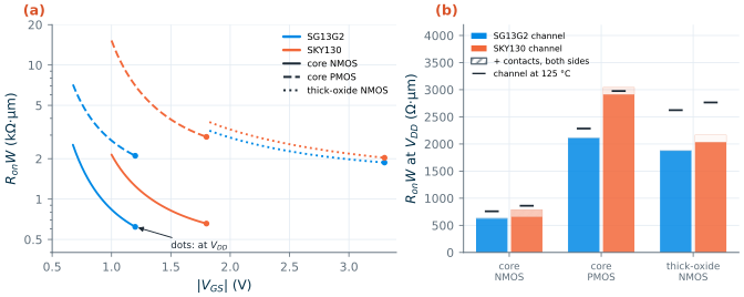
The contacts are where the PDKs differ most. Magic’s extraction files give 17 Ω for an SG13G2 diffusion contact, but 185 Ω for a SKY130 licon on n-diffusion plus 9.3 Ω for the mcon above it [20]. At the generators’ contact pitch (0.36 and 0.34 µm) that is 6.1 Ω·µm per side in SG13G2 and 66 Ω·µm per side in SKY130: 2 % of the channel resistance in one PDK, 20 % in the other. The SPICE model does not contain this term; it lives in the layout, and it is the reason a SKY130 power device wants contacts as close as the rules allow along every finger.
Metal debiasing and how current crowds
The metal fingers and buses are resistors too. Current enters the drain bus, spreads into the drain fingers, crosses the channel, collects in the source fingers and leaves through the source bus. Every metal drop subtracts from the voltage across part of the channel, so that part carries less current: the metal debiases the transistor. Two questions follow: how much resistance the metal adds, and how unevenly the current flows.
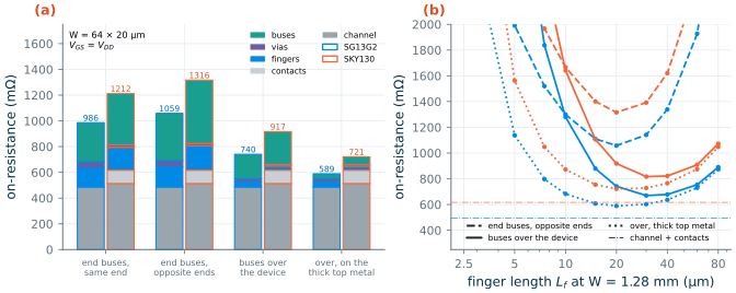
tools/figs/_ch29_debias.py answers both by brute force. It cuts each of the \(N+1\) source and drain fingers into 40 segments, connects neighbouring fingers through the channel conductance of Eq. (29.1) plus the contacts, links the segments of each finger by its metal resistance, adds the vias, and models the buses either as resistor lines outside the device or as two resistive sheets over it. The network has about 5 000 nodes and is solved in a fraction of a second. Figure 29.3 shows the channel current density it finds for a transistor of 64 fingers of 20 µm (W = 1.28 mm) with three metallization patterns, and Figure 29.4a the resistance budget of each.
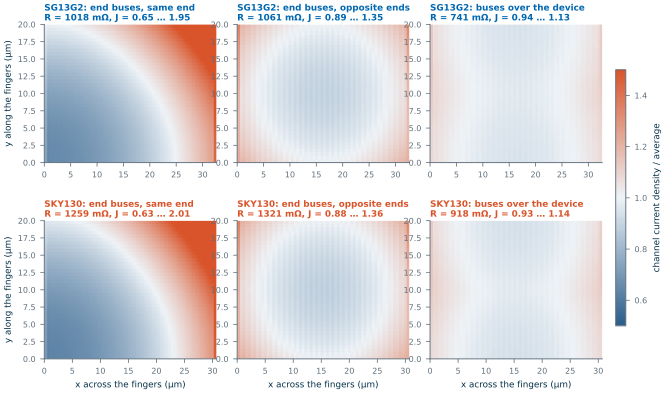
- End buses, terminals at the same end. The current takes the shortest metal path, crowding into the fingers close to the terminals and into the fed end of each finger, and the far corner carries 0.65 of the average while the near corner carries 1.95. This pattern has the lowest resistance of the two end-bus patterns, precisely because the current avoids the long metal paths; the price is a hot corner, a local current density twice the average for electromigration, and a device whose far half does little [61].
- End buses, terminals at opposite ends. Feeding the drains from one end and the sources from the other balances the path lengths: every element sees roughly the same total metal, the density stays within 0.89 to 1.36, and the resistance is a few per cent higher.
- Buses over the device. Each finger is fed along its own half, so its metal carries current over half the distance, and the bus is a wide sheet rather than a 5 µm strip. The metal resistance drops from 0.57 to 0.25 Ω in SG13G2 and the current stays between 0.94 and 1.14 of the average.
The hand formulas
Two results cover the uniform case. A metal finger of sheet resistance \(R_\square\), width \(w\) and length \(L_f\) that is fed at one end and loses its current evenly along its length dissipates as much as a resistor of one third of its end-to-end value; a finger fed evenly along one half, as under a bus over the device, as much as one twelfth. A bus of length \(X\) and height \(H\) that collects evenly along its length and leaves at one end behaves like one third of its end-to-end resistance:
Key equation · Metal resistance of a large transistor with uniform current
\[R_{finger} = \frac{R_\square L_f}{3w}\ \text{(fed at one end)}, \qquad \frac{R_\square L_f}{12w}\ \text{(fed along one half)}, \qquad R_{bus} = \frac{R_{\square,b}X}{3H}. \tag{29.4}\]With \(N/2\) drain fingers in parallel and as many source fingers, the fingers add \(2 \cdot R_{finger}/(N/2)\), the two buses \(2R_{bus}\).
Derivation · One third and one twelfth, from the dissipated power
The resistance seen at the terminals is the one that dissipates the same power at the same current, \(R = P/I^2\). Let a finger carry a total current \(I\), fed at \(y = 0\), and let the channel draw it evenly, \(I/L_f\) per unit length. At position \(y\) the metal still carries \(I(1 - y/L_f)\), so
\[P = \int_0^{L_f} I^2\left(1 - \frac{y}{L_f}\right)^2 \frac{R_\square}{w}\,dy = I^2\frac{R_\square L_f}{w}\cdot\frac{1}{3}.\]Under a bus over the device, the vias inject the current evenly along one half (rate \(2I/L_f\)) while the channel draws it evenly along the whole finger (rate \(I/L_f\)). In the fed half, at a distance \(s\) from its outer end, the metal carries \(sI/L_f\); in the other half the current \(I/2\) that crossed the middle runs down to zero. Each half dissipates \(\int_0^{L_f/2} (sI/L_f)^2 (R_\square/w)\,ds = I^2R_\square L_f/(24w)\), together \(I^2R_\square L_f/(12w)\). The bus result is the first integral with \(L_f\), \(w\) replaced by \(X\), \(H\). If the terminals of both buses sit at the same end or at opposite ends, the sum of the two integrals is the same to first order; only the distribution differs (Figure 29.3).
The formulas hold while the metal drop is small next to the channel drop. Their range is set by a characteristic length: for a pair of fingers with metal resistance \(r' = R_\square/w\) per unit length and channel conductance \(2/(R_{on}W + 2R_cW)\) per unit length between them, the current redistributes over \(\lambda \approx \sqrt{(R_{on}W + 2R_cW)/(4r')}\), which is 20 µm in both PDKs for first-metal fingers of 0.29/0.26 µm. Fingers much longer than \(\lambda\) conduct mainly near their fed end; the end-bus curves of Figure 29.4b turn up beyond \(L_f\) ≈ 20 µm for that reason [61].
Worked example 29.1 · The on-resistance of a 1.28 mm switch, by hand and with the network model
64 fingers of 20 µm at the generators’ pitch (0.51 µm SG13G2, 0.48 µm SKY130), first-metal fingers 0.29/0.26 µm wide, second-metal buses (\(R_\square\) = 0.088/0.125 Ω/□), VGS = VDD, 27 °C.
SG13G2. Channel: 621 Ω·µm / 1280 µm = 485 mΩ; contacts 2 × 6.1 / 1280 = 10 mΩ. End buses (5 µm wide): fingers \(2 \times (0.110 \times 20/(3 \times 0.29))/32\) = 158 mΩ, buses \(2 \times 0.088 \times 32.6/(3 \times 5)\) = 383 mΩ; total 1.036 Ω (model: 1.061 Ω with terminals at opposite ends, 1.018 Ω at the same end). Buses over the device (\(H\) = 10 µm): fingers 40 mΩ, buses \(2 \times 0.088 \times 32.6/30\) = 192 mΩ, total 0.726 Ω (model 0.741 Ω, the difference being the vias). The same buses on TopMetal1: 0.573 Ω (model 0.589 Ω).
SKY130. Channel 657/1280 = 513 mΩ; contacts 2 × 66/1280 = 104 mΩ. End buses: fingers 200 mΩ, buses 512 mΩ, total 1.329 Ω (model 1.321 Ω). Buses over the device: 50 + 256 mΩ, total 0.923 Ω (model 0.918 Ω). On met5: 0.726 Ω (model 0.721 Ω).
What it means. The hand formulas land within 3 % of the network for every evenly fed pattern; with both terminals at the same end the crowding they ignore lowers the true resistance by 2 % (SG13G2) and 5 % (SKY130). With simple end buses the metal adds more than the silicon; buses over the device halve that, and moving them to the thick top metal leaves 104 mΩ (SG13G2) and 208 mΩ of contacts plus metal (SKY130). The last 20 % in SKY130 is its contacts, which no metal pattern removes.
Current density and the other limits
The uniform result also tells where electromigration bites. With buses over the device each finger carries \(I/(N/2)\) at the edge of its bus; at 0.5 A through the 1.28 mm switch that is 16 mA per finger, far beyond the 0.36 mA a minimum SG13G2 Metal1 line may carry at 105 °C (Table 24.2). A first-metal finger therefore never carries the whole current along its length; the vias must hand it up within a short distance, and the finger metal is often doubled by a second metal stripe on top of it. Check the current density at three places: where each finger leaves its bus, in the vias of one finger (16 mA needs 40 Via1 cuts at 0.4 mA each in SG13G2), and at the narrowest point of each bus [15].
Power bipolar transistors are the other kind of large device. Of the bipolars in the two PDKs (Chapter 28), only SG13G2’s HBTs carry milliamperes, and only per emitter. Parallel emitters share current only if none of them runs away thermally: a hotter emitter has a lower VBE, draws more current and heats further. For one emitter with thermal resistance \(R_{th}\), temperature coefficient \(\varphi = \vert dV_{BE}/dT\vert\) and an emitter resistance \(R_E\), the electrothermal loop gain at collector current \(I\) is
\[G = \frac{I\,V_{CE}\,R_{th}\,\varphi}{nV_T + IR_E}, \tag{29.5}\]and the emitter is stable for \(G < 1\). For npn13G2 with one emitter (\(R_{th}\) = 11.4 kK/W, \(\varphi\) ≈ 1.4 mV/K, Chapter 24) at \(V_{CE}\) = 1.2 V the numerator is 19 Ω × \(I\); at 1 mA the denominator \(nV_T\) = 26 mV keeps \(G\) = 0.73 without ballast, but at 5 mA an emitter resistor of at least 14 Ω is needed. This is the bipolar version of debiasing, used on purpose: a ballast that drops two to three thermal voltages evens out emitters that see slightly different temperatures or metal drops [61]. SKY130’s bipolars are not meant for current; its power devices are MOS, including the 5 V gate, 10.5 V drain nfet_g5v0d10v5 of Figure 29.2 and a 16 V drain-extended variant (g5v0d16v0) in its model library [19].
29.3 Minority-carrier injection and guard rings
Where power devices inject
Chapter 24 treated latch-up and the taps and guard rings against it; this section looks at the trigger that power devices supply. A low-side NMOS that switches an inductive load sees its drain pulled below ground when it turns off: the drain–substrate junction becomes forward-biased and injects electrons into the substrate, as much current as the inductor demands. A high-side PMOS whose drain is pulled above its supply injects holes into its n-well, and the substrate PNP of Chapter 28 delivers most of them to the substrate as majority-carrier current. The ESD diode from VSS to a pad does the same whenever the pin goes below ground. The holes are the easy case: they raise the substrate potential near the injector, and substrate ties next to it (majority-carrier guard rings) return them. The electrons are the hard case. They are minority carriers in the p-substrate, they move by diffusion, and any n-region they reach, the n-well of a PMOS, a floating node, a photodiode, collects them as a current.
How far they travel is set by the diffusion length \(L_n = \sqrt{D_n\tau_n}\). With \(D_n \approx\) 30 cm²/s in a lightly doped substrate and a lifetime of 1 to 10 µs, \(L_n\) is 55 to 175 µm: comparable to the size of an analog block.
How much reaches a victim
tools/figs/_ch29_inject.py solves the diffusion equation \(\nabla^2 n = n/L_n^2\) in a cross-section through long parallel stripes: a 20 µm wide n+ drain at the surface held at the injecting concentration, a victim n-well 1.5 µm deep at a distance \(d\), and optionally an n-well guard ring tied to a supply between them, all as absorbing regions; the rest of the surface and the bottom of a 200 µm substrate reflect. It is a diffusion model, not a device simulation: no fields, no high injection, no resistance in the ring. Figure 29.5 shows the result.
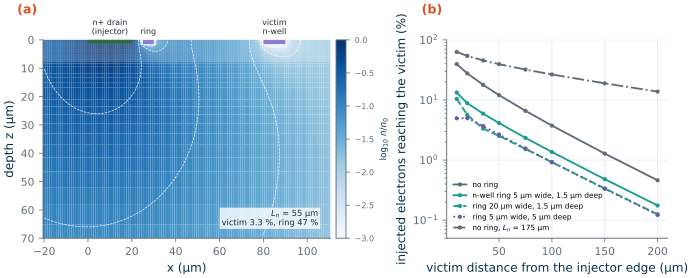
Without a ring, a victim 50 µm away collects 12 % of the injected electrons and one 100 µm away 3.7 %. A 5 µm n-well ring 1.5 µm deep collects 47 % of them and cuts the victim’s share by a factor of 2.7 to 3; making the ring four times wider or three times deeper gains another factor of 1.5. The ring cannot do better because it is shallow next to \(L_n\): electrons that start downwards pass under it and come up on the other side. This is why Hastings judges n-well electron collectors in CMOS of limited effect and prefers wide n+ or deep collectors, tied to a supply rather than to ground so that their own resistance does not debias them [61]. The diffusion length weighs even more: with \(L_n\) = 175 µm the unprotected victim at 100 µm collects 27 %.
Put numbers to it. A low-side switch that clamps 50 mA of inductive flyback for a few hundred nanoseconds injects about that much; 3.7 % of it, 1.9 mA, reaches an n-well 100 µm away without a ring and 0.7 mA with one. Chapter 24 found that 0.17 mA into the substrate latches an inverter whose ties sit at the rule limit, and 6 mA one surrounded by guard rings. The power device needs its own collector ring, distance, and guard rings around every CMOS block nearby.
What this means for your design
Treat every junction that can be forward-biased by a pin or an inductive load as an injector: power drains, ESD diodes to VSS, the cathodes of clamps. Surround it with an electron-collecting ring (n-well with as much n+ as possible, tied to a supply), put ties for the majority current next to it, and place the sensitive circuits far away, measured in diffusion lengths, not in micrometres. SKY130’s deep n-well gives a deeper collector than a plain n-well; whatever you use, its depth relative to \(L_n\) sets its efficiency.
29.4 ESD: events, models and requirements
The events
Electrostatic discharge (ESD) is the transfer of charge between bodies at different potentials. For a chip it happens during handling, assembly and test, mostly before it is ever powered, and it is far larger than any operating current. Two test models describe the events that matter:
- Human-body model (HBM). A charged person touches a pin while another pin is grounded. The tester stores the charge on 100 pF and discharges it through 1.5 kΩ into the device. Because the network inside the chip is a few ohms, the current is set by the tester: about \(V_{HBM}\)/1.5 kΩ, 1.3 A per 2 kV, rising in a few nanoseconds and decaying with a time constant of about 150 ns [134].
- Charged-device model (CDM). The package itself is charged, by sliding down a tube or through an electric field, and discharges when one pin touches ground. The source is the device’s own capacitance, a few picofarads, discharged through the pin and the path inside the chip in about a nanosecond. A 5 pF package at 500 V holds 2.5 nC; delivered in 1 ns that is several amperes, now flowing out of the chip through whatever path is shortest to the touched pin [135, 70].
The older machine model has been withdrawn; HBM and CDM are the two classifications a datasheet quotes, typically a few kilovolts HBM and a few hundred volts CDM [134, 135]. CDM is the harder one for layout, because its current is fast enough that the inductance and resistance of every wire between a pin and its protection decide what voltage a gate oxide sees.
What the protection must do
An ESD network has a window to fit in [61, 70]:
- Stay off in operation. No conduction, little leakage and little capacitance at any voltage the pin sees in normal use, including power-up and power-down in any order.
- Turn on in time and clamp low enough. During the event the voltage at every protected node must stay below what breaks it: the gate oxide (a few volts for a core device, Table 24.1), junction breakdown (about 12 V in both PDKs), and the drain breakdown of transistors connected to the pin.
- Survive. The protection devices and the metal must carry the current without melting, and must not latch into a state that the supply can sustain afterwards.
Devices are characterized for this with a transmission-line pulse (TLP): rectangular pulses of 100 ns and increasing amplitude, each followed by a leakage measurement, give the quasi-static I–V curve of the protection up to its failure current [70]. Figure 29.8b emulates it with a 100 ns current ramp on the PDK models.
The architecture
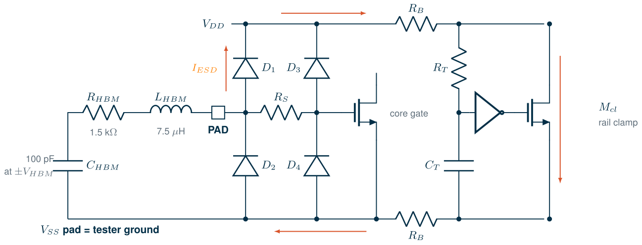
Figure 29.6 shows the network the I/O libraries of both PDKs use, the rail-based scheme of Chapter 17. Each pad has a diode to each rail. A positive strike from a pad to VSS forward-biases \(D_1\) and lifts the VDD rail; the rail clamp, a very wide NMOS between VDD and VSS, carries the current down. The clamp is turned on by the fast edge, not by a voltage: \(R_T\) and \(C_T\) hold the inverter’s input low for a time \(R_TC_T\) after the rail jumps, the inverter drives the clamp gate high, and the clamp conducts until the capacitor has charged [133]. In normal operation the supply ramps up over microseconds to milliseconds, \(C_T\) follows, and the clamp stays off. A negative strike forward-biases \(D_2\) directly. A strike between two pads goes through one diode, the rails and the clamp, and a strike between VDD and VSS through the clamp alone. Sensitive gates get a secondary stage: a series resistor \(R_S\) and small diodes close to the gate, which take the fast CDM current locally.
29.5 ESD protection structures in SG13G2 and SKY130
What each PDK ships
Neither PDK expects you to design ESD devices from scratch; both ship protected I/O cells, and SG13G2 also ships ESD devices as PyCells. Table 29.1 lists what is there and, as important, what is characterized.
Table 29.1. ESD devices, cells and models in IIC-OSIC-TOOLS 2026.10 [14, 20, 19].
| Quantity | SG13G2 | SKY130 |
|---|---|---|
| ESD device generators | PyCell esd: diodevdd_2kv/_4kv, diodevss_2kv/_4kv, nmoscl_2/_4 |
none (protection is inside the I/O cells) |
| ESD diode models | sg13g2_esd.lib: level-1 diodes with series resistance and breakdown (35 and 70 µm²) |
diode_pw2nd_11v0, diode_pd2nw_11v0 (with series resistance; _no_rs variants) |
| ESD transistor models | none (clamps use sg13_hv_nmos) |
esd_nfet_g5v0d10v5, esd_pfet_g5v0d10v5: BSIM4 cards (level 54), no snapback |
| Analog pad | sg13g2_IOPadAnalog: 2 × 27.8 × 1.26 µm diodes to each rail, gate-grounded NMOS (88 µm) and PMOS (266 µm) clamps, 587 Ω + small diodes as secondary protection |
sky130_ef_io__analog_esd_pad: 5 + 5 diodes of 50 µm² to VSSIO/VDDIO; minesd 1 + 1; noesd none |
| Rail clamp | in IOPadVdd, IOPadIOVdd: RC trigger (136 kΩ rppd, 2 × 63/9.5 µm MOS capacitor), inverter, 172 × 4.4/0.6 µm sg13_hv_nmos (757 µm) |
in sky130_fd_io__top_power_hvc_wpadv2: RC trigger (2720 µm res_generic_po), MOS capacitors, inverter, 2620 µm nfet_g5v0d10v5 |
| Snapback, failure current, HBM/CDM rating | not modelled, not published in the PDK files | not modelled, not published in the PDK files |
Figure 29.7 shows SG13G2’s ESD PyCells. The two diodes are long interdigitated stripes of n+ and p+ inside guard rings, 17.8 × 37 µm each; nmoscl_4 is a 69 × 24 µm multi-finger NMOS with a ring. Their names carry the HBM level they are meant for, and the 70 µm² of the 4kv diodes equals the 2 × 35 µm² of the diodes in every sg13g2_io pad.
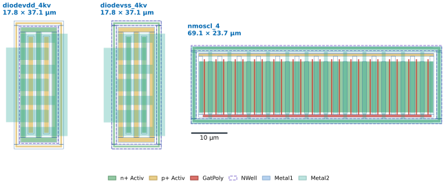
esd with model = diodevdd_4kv, diodevss_4kv and nmoscl_4; contacts and vias hidden, first metal as outlines. Generated by tools/layout/ch29/power_layouts.py.Common pitfall · Simulating ESD with models that were never meant for it
Three traps sit in the PDK files. The diodes in SG13G2’s I/O netlist,
dantennaanddpantenna, are fitted for reverse bias only (DC range −15 to 1 V); their forward series resistances are kilohms, so a simulation of the pad with them shows the diodes doing nothing. SKY130’sef_ioanalog-pad netlist writes the diode areas and perimeters in picometre units (area=5e+13), which ngspice reads as square metres: the diodes become ideal. And no MOS model in either PDK contains drain avalanche or the parasitic bipolar transistor that makes a clamp snap back, nor any failure current. Our simulations therefore use the ESD diode models ofsg13g2_esd.libfor SG13G2, the SKY130 diodes with their areas corrected to 50 µm² and 102 µm perimeter, and the rail clamps rebuilt device by device from the I/O netlists (the SG13G2 cell as written stalls ngspice’s transient solver; both are rebuilt the same way), and they are valid only while every transistor stays below its breakdown.
A simulated discharge
_ch29_sim.py builds the network of Figure 29.6 for an unpowered chip with its VSS pad grounded: the HBM tester with 7.5 µH of series inductance for a realistic rise, each PDK’s pad diodes, the rails as two ideal resistors \(R_B\) (0.1 Ω or 1 Ω each, standing for the metal between pad and clamp), and each PDK’s rail clamp with its trigger. The secondary stage is left out. Figure 29.8 shows what happens.
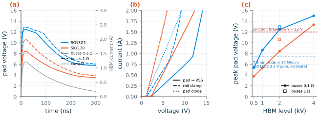
- The current is the tester’s. Both PDKs see a peak of 1.21 A at 2 kV, set by the 1.5 kΩ and the inductor; the chip’s few ohms do not matter.
- SKY130 holds the pad at 8.4 V. Five diodes in parallel (2.4 Ω dynamic resistance) and a 2620 µm clamp (2.5 Ω) share the voltage almost equally, and the clamp’s drain stays at 4.2 V, well inside the 10.5 V rating of
nfet_g5v0d10v5. - SG13G2’s pad reaches 12.5 V. Its diode model has 4.2 Ω of dynamic resistance, and its 757 µm clamp needs 7.1 V at its drain for 1.2 A through the channel alone. The sum would be 13.7 V; the pad stops at 12.5 V because the VSS-side diode breaks down at 11.3 V and takes part of the current straight to VSS. The clamp’s 7 V lies above the 5.3–6.3 V drain breakdown of the 3.3 V devices, so in silicon the clamp would avalanche and snap back here; the model is valid up to about 1 kV (5.0 V at the clamp), where the pad sees 8.6 V.
- Negative strikes are easy. The diode to VSS conducts directly: −4.6 V (SG13G2) and −5.6 V (SKY130).
- The rails matter. One ohm in each rail raises the 2 kV peak by 2.2 V in SKY130 (8.4 → 10.6 V). In SG13G2 it rises by only 0.5 V, because the breakdown of the VSS diode is already limiting.
Worked example 29.2 · The pad voltage of a 2 kV strike, by hand
Current. \(I_{pk} \approx V_{HBM}/R_{HBM}\) = 2000/1500 = 1.33 A; the series inductor of the tester lowers the simulated peak to 1.21 A.
SKY130. Pad diodes: five
pd2nw_11v0of 50 µm², each with \(R_S\) = 600 Ω·µm² / 50 µm² = 12 Ω, together 2.4 Ω; with about 1.1 V across the junction at this current, \(V_{D1}\) ≈ 1.1 + 1.21 × 2.4 = 4.0 V (TLP ramp: 4.05 V at 1.2 A). Clamp: 4.1 V at 1.2 A from its TLP curve. Rails: 2 × 0.1 Ω × 1.21 A = 0.24 V. Sum 8.3 V; the transient gives 8.43 V.SG13G2.
diodevdd_4kv: \(R_S\) = 289.6/70 = 4.1 Ω, so \(V_{D1}\) ≈ 1.0 + 1.21 × 4.1 = 6.0 V (TLP: 6.02 V). Clamp 7.5 V (TLP at 1.2 A), rails 0.24 V: sum 13.7 V. The transient gives 12.46 V: the sum exceeds the 11.3 V breakdown ofdiodevss_4kv(its \(R_S\) = 200/70 = 2.9 Ω), which opens a parallel path from the pad straight to VSS.What it means. The pad voltage is the sum of the series drops at the tester’s current, so every element of the path, diode, metal and clamp, needs a resistance budget. A thick-oxide gate on a SKY130 pad survives this in simulation; in SG13G2 the simulation leaves the models’ range, and the 3.3 V oxide (7.5 nm, about 7.5 V at 10 MV/cm) needs the clamp’s snapback, which the models do not show, or a second, wider clamp.
SG13G2 vs SKY130 · ESD protection you can use
SG13G2 SKY130 Ready-made pads sg13g2_io: analog, input, output (4/16/30 mA), supply and corner cells, 80 × 180 µmsky130_fd_io(SkyWater GPIO, power and analog pads) and Efablessef_iowrappers, 75 × 200 µmBuilding your own ESD PyCells and their diode models not supported: use the I/O cells Rail clamp 757 µm 3.3 V NMOS, RC 0.75 µs 2620 µm 5 V/10.5 V NMOS Simulated 2 kV HBM, pad to VSS 12.5 V (clamp beyond its breakdown) 8.4 V In both PDKs, use the I/O cells for every pin and keep the pad ring unbroken, so that the rails and clamps of all cells act together. For an analog pin, choose between the protected and the unprotected pad consciously (Chapter 17), and if you add your own protection in SG13G2, build it from the PyCells and check the pad voltage against what the pin’s gates can stand.
The SG13G2 trigger time constant follows from the cell netlist: 26 × 5.24 kΩ of rppd with two 63 × 9.5 µm thick-oxide MOS capacitors (4.6 fF/µm² for 7.5 nm, 5.5 pF) gives \(R_TC_T\) ≈ 0.75 µs, five times the HBM decay and a thousand times shorter than a supply ramp of a millisecond. In SKY130 the trigger resistor is 397 kΩ of res_generic_po (48.2 Ω/□).
29.6 Pad cells and their layout
The cells
Figure 29.9 shows the four cells of the simulation as the PDKs’ GDS libraries contain them. In SG13G2’s IOPadAnalog the bond pad itself is not part of the cell (the pad-ring generator places it); the cell holds the diodes, the gate-grounded clamps and the secondary stage, arranged from the pad end towards the core, with guard rings around the injecting devices. IOPadIOVdd is almost entirely its rail clamp: the 757 µm NMOS, the MOS capacitors and the long rppd trigger resistor. In SKY130 the analog_esd_pad is the Efabless wrapper of a bare pad with its ten diode stripes, and top_power_hvc_wpadv2 the SkyWater power pad, whose RC-triggered clamp fills most of the cell under and beside the pad opening [14, 18].
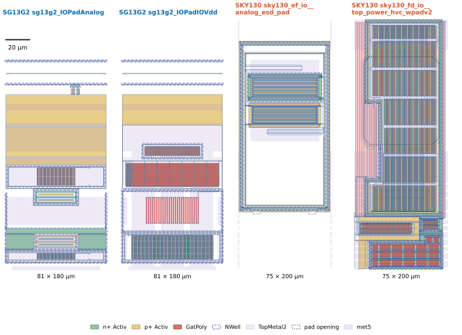
sg13g2_io.gds, sky130_ef_io__analog.gds and sky130_fd_io.gds; active, poly, n-well, top metal and pad opening shown, first metal as outlines, contacts and vias hidden.Layout rules for the ESD current path
The simulation turns into a short list of rules [61, 70]:
- Budget the resistance of the loop. The ESD current flows from the pad through a diode, along a rail, through a clamp and back along the other rail. Every ohm adds 1.2 V at 2 kV (Figure 29.8c). Hastings’s rule of thumb is a couple of ohms between any two pins at most; with the clamps above, 1 Ω per rail already costs 2 V. Run the rails in the thickest metals, stacked where possible: 1 mm of 20 µm wide TopMetal2 is 0.55 Ω in SG13G2, of met5 1.45 Ω in SKY130.
- Place clamps along the ring, not in one corner. The rail resistance between a pad and the nearest clamp is what counts, so a long pad ring needs several clamps; the I/O libraries put one in every supply pad for this reason, and the rails of all cells must abut without breaks [133].
- Make ESD metal wide enough not to melt. An HBM pulse lasts too short for the heat to leave a wire, so the wire must absorb it: with \(\int I^2dt = I_{pk}^2\tau/2\) for an exponential decay, a line of sheet resistance \(R_\square\), thickness \(t\) and width \(w\) heats by \(\Delta T = R_\square\int I^2dt/(c_vtw^2)\), with \(c_v\) = 2.42 J/(cm³·K) for aluminium. Table 29.2 gives the widths for a 300 K rise at 2 kV: several micrometres for the thin metals, 1 to 2 µm for the thick top metals, far more than electromigration asks for these currents’ average.
- Keep the path short and free of corners. Current crowds into the inside corner of a bend; chamfer the corners of ESD wires and run any stress slots along the current, not across it [61].
- Fence in the injectors. The diode to VSS, the clamps and the gate-grounded devices inject electrons whenever the pad goes below ground (Section 29.3); the I/O cells surround them with guard rings, and the core belongs at a distance behind the ring of pads.
- Put secondary protection next to the gate. The series resistor and the small clamps of the secondary stage protect against CDM only if they sit near the gate they protect and return to the same ground that gate’s source uses.
- Ballast output transistors. A multi-finger output NMOS on a pad is itself a clamp; if one finger snaps back first it carries the whole current. Silicide blocked over the drain or a resistor in series with each finger spreads the current, the ballasting of Section 29.2 used against failure [61].
Table 29.2. Minimum width of a wire that carries a whole 2 kV HBM pulse (1.33 A, τ = 150 ns) with an adiabatic temperature rise of 300 K, from the sheet resistances and thicknesses of Table 24.2 (tools/figs/ch29_numbers.json).
| SG13G2 layer | Width | SKY130 layer | Width |
|---|---|---|---|
| Metal1 (0.42 µm) | 6.9 µm | met1, met2 (0.36 µm) | 8.0 µm |
| Metal2–Metal5 (0.49 µm) | 5.7 µm | met3, met4 (0.845 µm) | 3.2 µm |
| TopMetal1 (2.0 µm) | 1.3 µm | met5 (1.26 µm) | 2.1 µm |
| TopMetal2 (3.0 µm) | 0.8 µm |
The widths scale linearly with \(V_{HBM}\), since \(w \propto I_{pk}\) at a fixed temperature rise. The estimate ignores the heat that flows into the oxide during the pulse, which makes it somewhat pessimistic for the thin metals, and it does not cover CDM, whose currents are larger but last a nanosecond.
Try it · Your own power switch and your own pad
In
tools/figs/ch29_power.py, changeNG, LF = 64, 20.0to the switch you need (for 0.25 Ω in SG13G2, about 2.6 mm of width) and runpython3 tools/figs/ch29_power.py debias sweep: which metallization pattern meets the target, and where is the optimum finger length now? Check one finger’s current against Table 24.2. Intools/figs/_ch29_sim.py, setRB = {"short": 0.1, "long": 2.0}and rerunpython3 tools/figs/_ch29_sim.py sky130andpython3 tools/figs/ch29_power.py hbm: how much rail resistance can the SKY130 pad tolerate before a thick-oxide gate on it is at risk? Finally, infig_inject()move the guard ring next to the victim instead of the injector (ring=(d - 10.0, 5.0, 1.5)): does it matter which side the ring is on?
- Large transistors are multi-finger arrays from the generators (pitch 0.51 µm in SG13G2, 0.48 µm in SKY130); the front end, not the metal, sets the pitch. Waffles lose their density advantage to the 45° metal rules here, and SG13G2 forbids their bent gates (Gat.f).
- RonW of the core NMOS at VDD is 621 Ω·µm (SG13G2) and 657 Ω·µm (SKY130), 22–31 % more at 125 °C; SKY130’s diffusion contacts add another 132 Ω·µm, SG13G2’s 12 Ω·µm.
- The metal adds as much as the silicon with simple end buses; the network model and the one-third/one-twelfth formulas agree within 3 % for evenly fed fingers. Buses over the device on a thick top metal bring a 1.28 mm switch to 0.59 Ω (SG13G2) and 0.72 Ω (SKY130), with current uniform within 6 %. Terminals at the same end lower the resistance but crowd the current twofold.
- Injected electrons diffuse over 55–175 µm; a shallow n-well ring catches about half of them and lowers what reaches a victim by about three times. Distance, ties and guard rings around every CMOS block do the rest.
- HBM delivers about 1.3 A per 2 kV for 150 ns, CDM several amperes for a nanosecond. With the PDKs’ own pad diodes and rail clamps a 2 kV strike reaches 8.4 V (SKY130) and 12.5 V (SG13G2) in simulation, but no model in either PDK covers snapback or failure, and none of the cells carries a published rating.
- Lay out the ESD loop as a power path: thick, wide rails (1 Ω per rail costs 2 V), clamps along the ring, several micrometres of metal against fusing, guard rings around the injecting devices, secondary protection next to the gate.
Further reading
- R. A. Hastings, The Art of Analog Layout [61]: Section 13.1 (power MOS transistors, their metallization, the rule of one-third and alternative layouts), Section 10.1 (power bipolar transistors and emitter ballasting), Section 14.2 (minority-carrier guard rings) and Section 14.4 (ESD devices and die-level protection, including the high-current metallization rules).
- A. Amerasekera and C. Duvvury, ESD in Silicon Integrated Circuits [70]: the physics of ESD devices, snapback and failure, TLP characterization and protection strategies.
- M.-D. Ker [133]: whole-chip protection with RC-triggered rail clamps, the scheme both PDKs’ I/O libraries use.
- The test standards, ANSI/ESDA/JEDEC JS-001 (HBM) [134] and JS-002 (CDM) [135], for the exact waveforms and classification levels.
- The I/O libraries themselves:
sg13g2_ioand the ESD PyCells and models of the IHP-Open-PDK [14], andsky130_fd_iowith its documentation [18].