Chapter 18
Switched-Capacitor Circuits
Replace a resistor by a capacitor and two switches, and the gain and time constants of a circuit become ratios of capacitors times a clock frequency. Both are far more accurate on a chip than any resistor. This chapter builds the switches, the clocks, an integrator and a gain stage around the course OTA, and measures what limits them in both PDKs.
- Explain how a switched capacitor behaves as a resistor, and why circuits built from capacitor ratios are accurate.
- Size a MOS switch from its on-resistance, and choose between NMOS, PMOS and transmission-gate switches in each PDK.
- Predict the charge injection and clock feedthrough of a switch, and the speed–accuracy trade-off they impose.
- Generate two non-overlapping clock phases, and explain why they must not overlap.
- Analyse the parasitic-insensitive integrator and the switched-capacitor gain stage, including the OTA’s finite gain and settling.
- Choose the sampling capacitor from the kT/C noise budget.
Contents
18.1 From resistors to switched capacitors
The amplifiers of Part IV set their gain with feedback, and a feedback network is usually made of resistors or capacitors. On a chip, neither has an accurate absolute value. A poly resistor’s sheet resistance is set by its doping and changes with temperature: the SG13G2 rhigh resistor changes by −37 % from −40 °C to 125 °C (Table 14.2). A MIM capacitor depends on the thickness of its dielectric. An RC time constant built from the two therefore has a tolerance of tens of per cent. What a chip does make accurately is a ratio of two components drawn from identical unit cells, laid out side by side (Chapter 15), and a frequency, from a crystal oscillator.
A switched capacitor turns a resistor into exactly those two quantities. In Figure 18.1b, switch \(\phi_1\) connects the capacitor to \(V_1\) and charges it to \(CV_1\); then switch \(\phi_2\) connects it to \(V_2\) and leaves it holding \(CV_2\). Each clock period \(T = 1/f_s\) moves a charge \(C(V_1 - V_2)\) from one node to the other, an average current \(I = f_sC(V_1 - V_2)\), so the switched capacitor behaves like a resistor
\[R_{eq} = \frac{1}{f_s C}. \tag{18.1}\]The idea of filters built this way dates from the early 1970s [85], and the first MOS switched-capacitor filters appeared in 1977 [86, 87]. In a switched-capacitor integrator the time constant becomes \(R_{eq}C_2 = C_2/(f_sC_1)\): a capacitor ratio times the clock period, accurate to the matching of the capacitors and the precision of the clock.
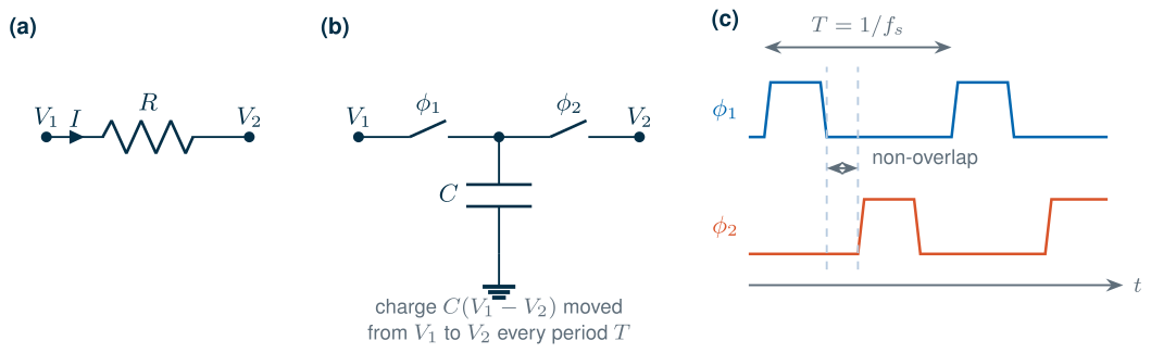
The equivalence holds only for signals that change slowly compared with the clock: a switched-capacitor circuit is a sampled-data circuit, which processes one sample per period. Its exact behaviour is described by difference equations and the z-transform, and its input must be band-limited to below \(f_s/2\) to avoid aliasing. Every circuit in this chapter is analysed sample by sample.
18.2 The MOS switch
A switch is a MOSFET in triode with a small drain-source voltage. With its gate at \(V_{DD}\) and its source and drain at the signal voltage \(V_{in}\), an NMOS switch has the on-resistance of Eq. (4.4) at small \(V_{DS}\),
\[R_{on} = \frac{1}{\mu_nC_{ox}(W/L)\,(V_{DD} - V_{in} - V_{TH})}. \tag{18.2}\]Its resistance rises as the signal rises, and the switch opens when \(V_{in}\) approaches \(V_{DD} - V_{TH}\). The threshold makes matters worse: the switch’s source is at \(V_{in}\) while its body is at ground, so the body effect raises \(V_{TH}\) as \(V_{in}\) rises. A PMOS switch, gate at 0 and body at \(V_{DD}\), behaves as the mirror image and conducts only near the top of the range. The transmission gate, an NMOS and a PMOS in parallel with complementary gate signals, covers the whole range if the two conduction regions overlap.
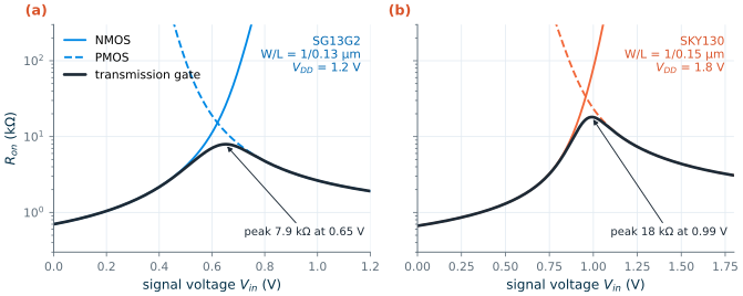
Figure 18.2 shows the on-resistance of minimum-length switches, 1 µm wide, simulated in both PDKs. Each NMOS starts at about 0.7 kΩ at \(V_{in}\) = 0, but the SG13G2 NMOS is practically off (above 100 kΩ) at 0.72 V and the SKY130 NMOS at 1.02 V. The PMOS devices conduct down to 0.50 V and 0.86 V. The transmission gate’s resistance peaks where the two devices hand over: 7.9 kΩ at 0.65 V in SG13G2 and 18 kΩ at 0.99 V in SKY130.
SG13G2 vs SKY130 · Where the transmission gate is weakest
Both PDKs have the same NMOS on-resistance at the bottom of the range, but they differ in the middle. In SG13G2 the NMOS and PMOS conduction regions overlap by more than 0.2 V (from 0.50 to 0.72 V), so the transmission gate never exceeds 7.9 kΩ·µm. In SKY130 the overlap is narrower (0.86 to 1.02 V), the NMOS has a stronger body effect (\(\gamma\) = 0.41 against 0.23 V½, Table 4.2) and the PMOS is weak, so the peak is 18 kΩ·µm, 2.3 times higher, in spite of the larger supply. A SKY130 transmission gate needs a wider PMOS for the same worst-case resistance, or a switch whose gate voltage follows the signal: the bootstrapped switch of Chapter 19.
In a switched-capacitor circuit, the switches that connect to the OTA’s virtual ground or to \(V_{CM}\) always see the same voltage, and their resistance is constant. Only the switches at the input see the full signal swing. A resistance that changes with the signal makes the sampling time constant signal-dependent, which distorts a fast signal: Chapter 19 measures that distortion.
18.3 Charge injection and clock feedthrough
A switch is not ideal when it opens. While it is on, its channel holds a charge
\[Q_{ch} = WLC_{ox}\,(V_{DD} - V_{in} - V_{TH}). \tag{18.3}\]When the gate falls, this charge must leave the channel, through the source and the drain. The part that flows onto the hold capacitor \(C_H\) changes its voltage; this is charge injection. In addition, the gate’s falling edge couples onto \(C_H\) through the gate-drain overlap capacitance \(C_{ov}\); this is clock feedthrough. With a fast clock edge, each side of the channel receives about half of its charge [90, 91], and the voltage error, the pedestal, is
Key equation · Pedestal of an NMOS switch (fast clock edge)
\[\Delta V \approx -\frac{\tfrac12 Q_{ch} + C_{ov}V_{DD}}{C_H + C_{ov}}. \tag{18.4}\]Both terms are negative for an NMOS switch: the falling gate pulls the hold capacitor down. The channel term depends on the signal through \(V_{in}\) and \(V_{TH}\); the feedthrough term does not.
Figure 18.3a compares Eq. (18.4), with \(Q_{ch}\), \(V_{TH}\) and \(C_{ov}\) taken from the simulator’s operating point, with transient simulations of a 1 µm switch on 100 fF, opened by a gate edge of 100 ps. The pedestal is between −9 and −4.5 mV, and the equation is within about 15 % in both PDKs. The PDKs differ in its composition. At \(V_{in} = V_{DD}/4\), the SG13G2 switch has an intrinsic gate capacitance of 0.67 fF and an overlap of 0.64 fF per side, so clock feedthrough provides 85 % of its pedestal of −8.4 mV. The SKY130 switch (1.0 fF and 0.25 fF) gets 64 % of its −7.4 mV from feedthrough. A slower edge gives the channel time to drain back to the input source: with a 2 ns edge the pedestals fall to −7.0 and −5.7 mV.
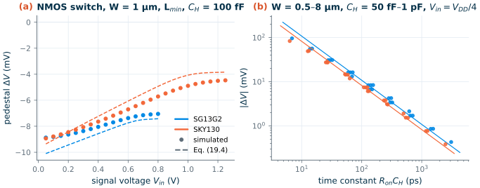
The second panel shows the trade-off behind every sampled-data circuit. Multiply the pedestal by the time constant \(\tau = R_{on}C_H\) with which the switch charges the capacitor:
\[\lvert\Delta V\rvert\cdot\tau \approx \left(\tfrac12 Q_{ch} + C_{ov}V_{DD}\right)R_{on}. \tag{18.5}\]The capacitor has cancelled, and since \(Q_{ch}\) and \(C_{ov}\) grow with \(W\) while \(R_{on}\) falls with it, so has the width. The product of speed and error is a property of the process: about 1.1 mV·ns in SG13G2 and 0.8 mV·ns in SKY130; the 25 combinations of width and capacitor in Figure 18.3b all lie within −40 % and +25 % of these values, the fastest switches lowest, because their channel partly drains back to the input during the 100 ps edge. A switch that charges its capacitor in 100 ps leaves a pedestal of about 10 mV; to reach 1 mV, accept 1 ns. If only the channel term counted, the product would be \(L^2/(2\mu)\), which is why short channels make fast, accurate switches; in SG13G2 the overlap term dominates.
How do circuits live with millivolts of pedestal? Three ways, all used later in this part:
- Make it signal-independent. The constant part, from feedthrough and from switches at fixed voltages, is an offset; a differential circuit, in which both halves receive the same pedestal, cancels it.
- Open the switch at a fixed voltage first. Bottom-plate sampling (Chapter 19) opens a switch at the virtual ground before the input switch, so the signal-dependent charge has nowhere to go.
- Compensate it. A half-size dummy switch, driven by the inverted clock, absorbs the charge the main switch releases; it works well only when the charge splits evenly.
18.4 Two non-overlapping phases
The two switches of Figure 18.1b must never be on at the same time: if they were, \(V_1\) would be connected to \(V_2\) through two small resistances, and the charge transfer would no longer be \(C(V_1 - V_2)\). In the integrator of the next section, an overlap would connect the input directly to the OTA’s virtual ground. The clocks therefore have a non-overlap gap between one phase falling and the other rising (Figure 18.1c).
The standard generator (Figure 18.4) cross-couples two NOR gates. Each phase can rise only after the other, delayed by two inverters, has fallen, so the gap is the delay of the inverters and the NOR gate. The inverters also buffer the phases, which drive the gates of many switches.
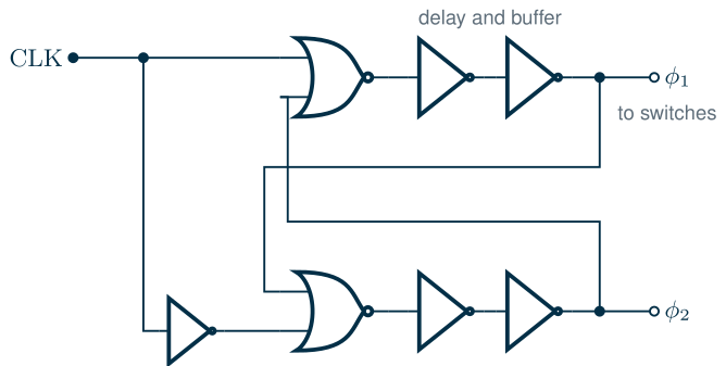
We built the generator from minimum-length core transistors of each PDK (NMOS 1 µm, PMOS 2 µm wide in the inverters, 4 µm in the NOR’s series PMOS) with 50 fF on each phase. Figure 18.5 shows the result: a non-overlap of 202 ps in SG13G2 and 241 ps in SKY130. Each additional pair of inverters adds 53 ps in SG13G2 and 47 ps in SKY130. A gap of a few hundred picoseconds costs nothing at a 1 MHz clock, but it must be larger than the skew between the clock wires that reach different switches; on a large chip, designers add delay for margin.
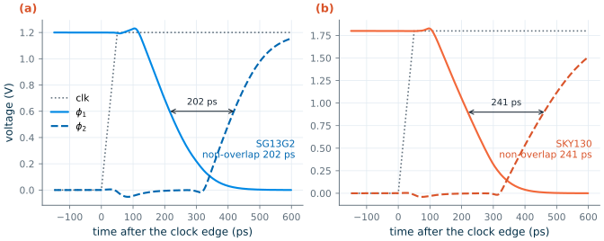
The rest of this chapter’s simulations use ideal clock sources with a 5 ns gap and 1 ns edges, so that the circuits, not the clocks, set the results.
18.5 The switched-capacitor integrator
Put the switched capacitor of Eq. (18.1) in place of the input resistor of an inverting integrator and you get the circuit of Figure 18.6a. It works, but it has a flaw: the node between the two switches carries not only \(C_1\) but also every parasitic capacitance \(C_p\) connected to it, the junctions and overlaps of both switches and the bottom plate of \(C_1\). All of it is charged to \(V_{in}\) and dumped into the integrator, so the gain becomes \((C_1 + C_p)/C_2\). Parasitic capacitances are neither accurate nor linear, and the circuit loses the very property that motivated it.
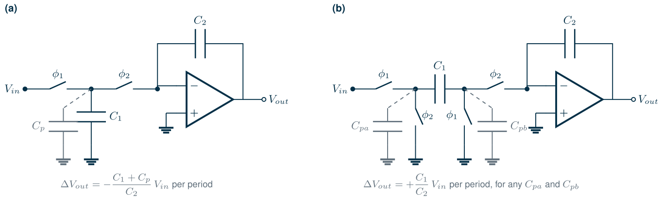
The parasitic-insensitive integrator of Figure 18.6b switches both plates of \(C_1\) [52, 92]. In phase 1, \(C_1\) charges to \(V_{in}\) with its right plate at ground. In phase 2 its left plate goes to ground and its right plate to the OTA’s virtual ground; the charge \(C_1V_{in}\) moves onto \(C_2\). The parasitic \(C_{pa}\) on the left plate is charged by the input and discharged to ground, and never reaches the virtual ground. \(C_{pb}\) on the right plate sits between ground and a virtual ground, so its voltage never changes and it carries no charge. Sample by sample (voltages relative to \(V_{CM}\)),
\[V_{out}[n] = V_{out}[n-1] + \frac{C_1}{C_2}\,V_{in}[n-1], \qquad H(z) = \frac{C_1}{C_2}\,\frac{z^{-1}}{1 - z^{-1}}. \tag{18.6}\]For signals far below \(f_s\), \(z^{-1} \approx 1 - s/f_s\) and \(H \approx (C_1/C_2)\,f_s/s\), an integrator with a unity-gain frequency of \(f_sC_1/(2\pi C_2)\). Swapping the phases of the two left-plate switches gives an inverting integrator without the delay \(z^{-1}\).
We built both integrators around the course OTA of Chapter 12 with \(C_1\) = 0.25 pF, \(C_2\) = 1 pF, transmission gates of 2 µm (NMOS) and 4 µm (PMOS), a 1 MHz clock and a constant input 40 mV above \(V_{CM}\): each period should add \(C_1/C_2 \times\) 40 mV = 10 mV. We then added \(C_p\) = 25 fF, a tenth of \(C_1\), to each switched plate. Figure 18.7 shows the result.
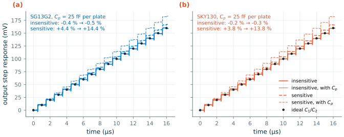
The parasitic-insensitive integrator stays within 0.5 % of \(C_1/C_2\) in both PDKs (−0.4 % in SG13G2, −0.2 % in SKY130), and the added parasitic changes its step by less than 0.1 %. The parasitic-sensitive one is wrong by +4 % even without the added capacitor, because the two switches’ junction and overlap capacitances add about 10 fF to its input node; with the extra 25 fF it is wrong by +14 %, exactly the ratio \(C_p/C_1\) more.
Common pitfall · Trusting a parasitic-sensitive structure
A circuit that works in a schematic with ideal switches can be several per cent off with real ones, because the switches themselves are parasitic capacitors. Check every node of a switched-capacitor circuit: if a node that carries signal charge also connects to a parasitic that is not reset to a fixed voltage in every phase, the circuit is parasitic-sensitive. Connect the bottom plate of each capacitor (the plate nearer the substrate, with the larger parasitic) to the low-impedance side, the input or the OTA output, never to the virtual ground.
18.6 The switched-capacitor gain stage
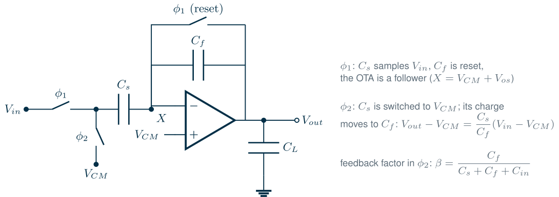
The most common switched-capacitor circuit is a gain stage that samples its input, multiplies it by a capacitor ratio and holds the result for the next circuit: the core of pipelined and algorithmic ADCs (Chapter 21). Figure 18.8 shows a version that also cancels the OTA’s offset. In phase 1, \(C_s\) samples \(V_{in}\) while the reset switch closes the OTA into a follower; node X then sits at \(V_{CM} + V_{os}\) and \(C_f\) is shorted. In phase 2, \(C_s\) is switched to \(V_{CM}\), and its charge moves to \(C_f\):
\[V_{out} - V_{CM} = \frac{C_s}{C_f}\,\frac{V_{in} - V_{CM}}{1 + 1/(\beta A_0)}, \qquad \beta = \frac{C_f}{C_s + C_f + C_{in}}. \tag{18.7}\]Because X starts each phase 2 at \(V_{CM} + V_{os}\), the OTA’s offset appears at the output only once, not multiplied by \(1 + C_s/C_f\). The finite gain of the OTA leaves a relative error of \(1/(\beta A_0)\), where \(\beta\) is the feedback factor in phase 2 and \(C_{in}\) the OTA’s input capacitance [88, 89].
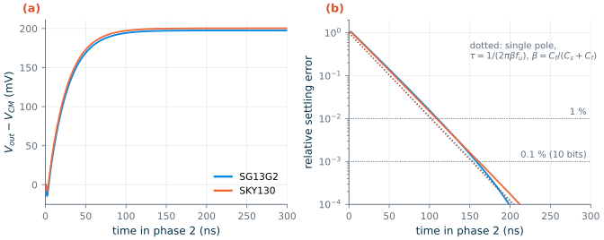
The output must also settle within phase 2. The OTA is now in a feedback loop with factor \(\beta\), so its loop gain crosses unity at about \(\beta f_u\), where \(f_u\) is the OTA’s unity-gain frequency. If the loop behaves like a single pole, the error falls as
\[\varepsilon(t) = e^{-t/\tau}, \qquad \tau = \frac{1}{2\pi\beta f_u}, \qquad t_N = \tau N\ln 2 \ \text{ for an error of } 2^{-N}. \tag{18.8}\]We simulated the stage with \(C_s\) = 1 pF, \(C_f\) = 0.5 pF (a gain of 2), a 1 pF load and inputs of \(V_{CM} \pm\) 100 mV, and took the difference of the two outputs, so that offsets and the constant part of the charge injection cancel (Figure 18.9). The gain is 1.9948 in SG13G2 and 1.9990 in SKY130, errors of −0.26 % and −0.05 %. Eq. (18.7) with the OTA gains of Chapter 12 (62.2 and 75.7 dB) and \(C_{in}\) = 0 predicts −0.23 % and −0.05 %; the small extra error in SG13G2 corresponds to an input capacitance of about 0.17 pF, from its large input pair (18.2 µm × 3 µm). The error then falls exponentially with a time constant of 21.4 ns (SG13G2) and 22.7 ns (SKY130), within 4 % of Eq. (18.8) with \(\beta = 1/3\) and \(f_u\) = 21.5 MHz (22.2 and 22.0 ns).
Worked example 18.1 · How fast can the course OTA clock a 10-bit gain stage?
Hand estimate. With \(\beta = 1/3\) and \(f_u\) = 21.5 MHz, Eq. (18.8) gives \(\tau\) = 22 ns. An error of \(2^{-10} \approx 0.1\) % needs \(t_{10} = 10\ln 2\,\tau = 6.9\tau\) = 153 ns. Phase 2 must be at least that long, plus two non-overlap gaps, so the clock period must be at least about \(2 \times 165\) ns: \(f_s \le\) 3 MHz.
Simulation. The stage of Figure 18.9 reaches 0.1 % at 158 ns in SG13G2 and 161 ns in SKY130. Slewing costs little here: the output step is 200 mV and the OTA slews at 15 V/µs or more (Chapter 12), so slewing takes at most about 13 ns.
What limits it. The settling time is set by \(\beta f_u = \beta\, g_{m1}/(2\pi C_c)\). Doubling the speed means doubling \(g_{m1}\) (twice the input-stage current in moderate inversion) or halving \(C_c\), which needs a higher second pole and so more current in \(M_6\) (Chapter 12). A larger gain lowers \(\beta\) and slows the stage in proportion. And the gain error must stay below the target too: 0.26 % in SG13G2 is already more than \(2^{-10}\), so a 10-bit SG13G2 stage needs more OTA gain, for instance a cascoded first stage.
18.7 kT/C noise sets the capacitor size
Every time a switch opens, it freezes a noise voltage of variance \(kT/C\) on its capacitor, independent of the switch resistance (Section 13.5). In a sampled-data circuit this noise is part of every sample, so the sampling capacitor must be large enough for the noise to stay below the resolution. A common target is to make the kT/C noise no larger than the quantization noise of an N-bit converter with a full-scale range \(V_{pp}\), whose step is \(V_{pp}/2^N\) and whose noise power is a step squared over 12 (Chapter 21):
\[\frac{kT}{C} \le \frac{1}{12}\left(\frac{V_{pp}}{2^N}\right)^2 \quad\Longrightarrow\quad C \ge \frac{12\,kT\cdot 4^N}{V_{pp}^2}. \tag{18.9}\]Every additional bit costs four times the capacitance, and with it four times the current for the same settling time. Table 18.1 evaluates Eq. (18.9) for a signal swing of half the supply in each PDK.
Table 18.1. Smallest sampling capacitor with kT/C noise equal to the quantization noise (Eq. 18.9, 27 °C), for a peak-to-peak swing of VDD/2.
| Resolution | SG13G2 (\(V_{pp}\) = 0.6 V) | SKY130 (\(V_{pp}\) = 0.9 V) |
|---|---|---|
| 8 bits | 9.1 fF | 4.0 fF |
| 10 bits | 145 fF | 64 fF |
| 12 bits | 2.3 pF | 1.0 pF |
| 14 bits | 37 pF | 16 pF |
What this means for your design
- A lower supply costs capacitance, and capacitance costs power. For the same resolution SG13G2 needs \((1.8/1.2)^2\) = 2.25 times the capacitance of SKY130, because its swing is smaller. A differential circuit doubles the signal swing for the same supply and divides the required capacitance by four, at twice the number of capacitors: one reason why precision switched-capacitor circuits are almost always differential.
- Below about 10 bits, other effects set the capacitor size. A 10 fF capacitor is smaller than the parasitic capacitance of its switches and wiring; matching (Chapter 15) and charge injection usually set a floor of 50–100 fF per unit.
- Size the switch last. Choose \(C\) from noise and matching, the OTA from settling, then the switch: wide enough that \(R_{on}C\) is a small fraction of the settling time, and no wider, because Eq. (18.5) says every bit of extra speed costs pedestal.
Try it · The switched-capacitor script
Every number in this chapter comes from
tools/figs/ch19_switched_cap.py, which runs its parts separately:python3 tools/figs/ch19_switched_cap.py integ amp. Try three changes. (1) Make the transmission gates four times wider (WN_SW,WP_SW): the sensitive integrator’s error without added parasitic grows, the insensitive one’s does not. (2) Run the gain stage at a 4 MHz clock (scamp(..., tclk=250e-9)): does it still settle to 0.1 %? (3) Replace the transmission gates at the virtual ground by single NMOS switches: in which PDK does that still work, and why (Figure 18.2)?
- A switched capacitor moves a charge \(C\Delta V\) per clock period and acts as a resistor \(1/(f_sC)\); gains and time constants become capacitor ratios and clock periods, which a chip makes accurately.
- A minimum-length transmission gate, 1 µm wide, has a worst-case on-resistance of 7.9 kΩ in SG13G2 (at 0.65 V) and 18 kΩ in SKY130 (at 0.99 V); SKY130’s narrow NMOS–PMOS overlap and weak PMOS make its switches harder to size.
- Charge injection and clock feedthrough leave a pedestal of a few millivolts on 100 fF, predicted within 15 % by Eq. (18.4). Pedestal times time constant is a process constant: about 1.1 mV·ns (SG13G2) and 0.8 mV·ns (SKY130).
- Two clock phases must never overlap; a cross-coupled NOR generator gives a gap of 0.2–0.24 ns with two inverters in each path.
- The parasitic-insensitive integrator delivers \(C_1/C_2\) within 0.5 % with the course OTA in both PDKs; the parasitic-sensitive one was 4 % off from its own switches alone.
- The switched-capacitor gain stage has a gain error of \(1/(\beta A_0)\) (−0.26 % and −0.05 % for the course OTA at a gain of 2) and settles with \(\tau = 1/(2\pi\beta f_u)\) = 22 ns, limiting a 10-bit stage to a clock of about 3 MHz.
- kT/C noise sets the sampling capacitor: four times more per bit, and 2.25 times more in SG13G2 than in SKY130 for the same resolution.
Further reading
- T. Chan Carusone, D. A. Johns and K. W. Martin, Analog Integrated Circuit Design [52], the chapters on switched-capacitor circuits and filters: z-domain analysis, the parasitic-insensitive building blocks and complete filter design.
- B. Razavi, Design of Analog CMOS Integrated Circuits [51], chapter 13 on switched-capacitor circuits, and his column on the switched-capacitor integrator [92].
- J. T. Caves et al. [86] and B. J. Hosticka, R. W. Brodersen and P. R. Gray [87]: the two papers that introduced MOS switched-capacitor filters.
- G. Wegmann, E. A. Vittoz and F. Rahali [91]: how the channel charge divides between source and drain, as a function of the clock edge and the impedances on each side.
- G. C. Temes [88] and K. Martin and A. S. Sedra [89]: the effect of the op amp’s finite gain and bandwidth on switched-capacitor circuits.