Chapter 26
Capacitors and Inductors
On-chip capacitors trade density against linearity and parasitics; on-chip inductors trade area against quality factor. This chapter measures both trades in SG13G2 and SKY130, with the devices drawn by the PDKs' own generators and characterized with their own models, and shows where the layout decides on which side of each trade a design lands.
- Compare MIM, MOM, MOS and varactor capacitors of both PDKs in density, linearity, leakage and parasitics, and choose one for a given job.
- Lay out MIM and fringe capacitors with a controlled bottom-plate and routing parasitic, and estimate that parasitic by hand.
- Read the C–V curve of a MOS capacitor and a varactor, and bias a MOS capacitor where its value is stable.
- Quantify voltage and temperature coefficients from the PDK documents and models, and translate them into distortion and drift.
- Estimate the inductance, series resistance, quality factor and self-resonance of a spiral inductor from its layout.
Contents
Chapter 3 gave the capacitance densities of both PDKs and extracted the area and perimeter coefficients of their MIM capacitors; the 3D gallery shows a MIM capacitor, a varactor and an inductor of each PDK as interactive models; Chapter 15 placed the Miller capacitor of the course OTA with its bottom plate on the output; Chapter 18 and Chapter 19 built switched-capacitor circuits and bottom-plate sampling on top of these devices. This chapter goes underneath: what each capacitor is made of, how large its parasitics are and which layout choices set them, how its value moves with voltage and temperature, and when a MOS capacitor can replace a MIM capacitor at a quarter of the area. A short section on spiral inductors closes it. Matching of capacitor arrays belongs to Chapter 27. The layouts come from IHP’s KLayout PyCells and Magic’s SKY130 generators, the numbers from the PDK documents and from ngspice runs of the PDK models in IIC-OSIC-TOOLS [35, 14, 20]:
python3 tools/layout/ch26/cap_layouts.py     # PyCells and Magic draw the devices; extraction, 3D models
python3 tools/figs/_ch26_sim.py              # capacitor and inductor simulations in both PDKs (about a minute)
python3 tools/figs/ch26_capacitors.py        # the figures and tools/figs/ch26_numbers.json
26.1 Capacitor types in a CMOS process
Every integrated capacitor is two conductors separated by an insulator. For plates of area \(A\) at a distance \(t\), with a dielectric of relative permittivity \(\varepsilon_r\),
\[C = \frac{\varepsilon_r\varepsilon_0 A}{t}, \tag{26.1}\]to which the field that bulges out at the plate edges adds a term proportional to the perimeter \(P\):
\[C = C_a A + C_p P, \tag{26.2}\]the area-plus-perimeter law of Chapter 3 with the area coefficient \(C_a = \varepsilon_r\varepsilon_0/t\). A process can therefore raise the density in only two ways: a thinner dielectric or a higher permittivity. Both cost something. A thin dielectric breaks down at a lower voltage and leaks; a high-permittivity material is usually less linear and less stable with temperature [61]. The four families of capacitors in SG13G2 and SKY130 sit at different points of that compromise:
- Metal-insulator-metal (MIM) capacitors add a thin deposited dielectric and an extra thin top plate above one metal layer, at the cost of one or two masks. SG13G2’s dielectric is 40 nm thick and gives 1.5 fF/µm², so by Eq. (26.1) its permittivity is about 6.8, that of silicon nitride [15]. SKY130 publishes 2.0 fF/µm² but not the dielectric [18]. Both electrodes are metal, so neither depletes: MIM capacitors are linear and stable, and they sit high in the stack, far from the substrate.
- Metal-oxide-metal (MOM) or fringe capacitors are combs of interleaved fingers in the ordinary interconnect layers. They need no extra mask; their field runs sideways between fingers, through the inter-metal oxide.
- MOS capacitors use the gate oxide, the thinnest dielectric in the process (2.65 nm in SG13G2’s core devices, 4.15 nm in SKY130’s): 13.0 and 8.3 fF/µm² at most. Their lower electrode is silicon, which depletes, so their value depends strongly on the voltage, and a thin oxide leaks.
- Varactors turn that voltage dependence into a feature: a MOS structure in an n-well, built to be tuned.
A plain plate of Metal2 over Metal1 is not in this list for a reason: across 0.54 µm of inter-metal oxide it gives only 68 aF/µm² (SG13G2 specification), twenty times less than the MIM capacitor [15]. Junction capacitors and poly–poly capacitors, which older processes offered, are not characterized in either PDK. Figure 26.1 shows the devices as their generators draw them, at one scale, and Table 26.1 summarizes what the rest of the chapter measures.
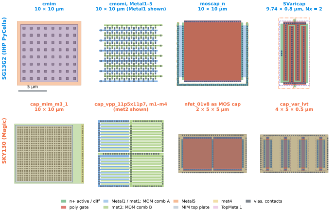
tools/layout/ch26/cap_layouts.py; layer colours as in the 3D gallery.Table 26.1. The capacitors of SG13G2 and SKY130: density at the typical bias, parasitic to the substrate (or shields) relative to the capacitance, coefficients and spread. Values from the PDK documents and from the simulations and extractions of this chapter [15, 14, 18, 19].
| Device | Structure | Density (fF/µm²) | Parasitic / C | Voltage coefficient | TC (ppm/K) | Spread |
|---|---|---|---|---|---|---|
SG13G2 cap_cmim |
Metal5 – 40 nm nitride – MIM plate, contacted from TopMetal1 | 1.5 + 0.04 fF/µm of edge | 1 % (1 pF) | −26 ppm/V, +5 ppm/V² (spec; not in model) | +3.6 | ±10 % |
SG13G2 cap_cmomi |
interdigitated combs, Metal1–Metal5 | 1.08 (5 layers, per footprint) | not modelled | none modelled | none modelled | not modelled |
SG13G2 cap_cmomf |
fringe combs, alternating direction per layer | 1.52 (5 layers) | not modelled | none modelled | none modelled | not modelled |
SG13G2 moscap_n, moscap_p |
core gate oxide, 2.65 nm | 12.7 at 1.2 V, 1.6 at 0 V | well junction (p) | 5.3 %/V at 1.2 V | −150 at 1.2 V | MOS corners |
SG13G2 SVaricap |
thick oxide over n-well, accumulation | 2.5 to 5.8 | well junction | tuning 2.3 : 1 over ±3 V | −240 at 0 V | MOS corners |
SKY130 cap_mim_m3_1, _m3_2 |
met3 – capm, met4 – cap2m; stackable | 2.0 + 0.19 fF/µm of edge | 1.2 % (1 pF) | not specified, not modelled | not modelled | ±10 % |
SKY130 cap_vpp_* |
fixed MOM cells, li1 to met5, optional shields | 0.55 to 1.42 | 7 to 14 % | none modelled | none modelled | about ±22 % |
SKY130 nfet_01v8, pfet_01v8 as capacitors |
core gate oxide, 4.15 nm | 7.9 at 1.8 V, 2.2 at 0 V | well junction (p) | 2.5 %/V at 1.8 V | −68 at 1.8 V | MOS corners |
SKY130 cap_var_lvt, _hvt |
core oxide over n-well, accumulation | 1.7 to 8.9 | well junction | tuning 5.2 : 1 (lvt) over ±2 V | none modelled | MOS corners |
26.2 MIM capacitors: density, parasitics and layout
Density and size
The SG13G2 MIM capacitor follows Eq. (26.2) with \(C_a\) = 1.5 fF/µm² and \(C_p\) = 40 aF/µm; its specification allows 1.35 to 1.65 fF/µm², and the corners cap_bcs and cap_wcs scale both terms by ±10 % [15, 14]. A single device may be 75 × 75 µm at most (rule MIM.g, 5625 µm²), and IHP recommends no more than 0.17 mm² of MIM per chip (MIM.gR) [16]. SKY130’s cap_mim_m3_1 has 2.0 fF/µm² (1.8 to 2.2) and a perimeter term almost five times larger, 0.19 fF/µm (0.11 to 0.27) [18]; its model also shrinks each side by 25 nm. Magic draws one cell up to 30 × 30 µm and arrays larger ones, and the second MIM layer above met4 (cap_mim_m3_2) can be stacked on the first for 4 fF/µm² over the same footprint (Figure 26.3a). The perimeter term matters only for small capacitors: at a side of 10 µm it adds 1 % in SG13G2 and 3.7 % in SKY130.
Which plate faces the substrate
A MIM capacitor is not symmetric. Figure 26.2 draws both to scale. The bottom plate is an ordinary metal plate (Metal5 in SG13G2, met3 in SKY130) that extends beyond the top plate, and below it there is nothing but oxide down to the substrate. The top plate is the thin MIM layer, contacted through a dense via array from the metal above (TopMetal1, met4); it sees only the bottom plate below it. Every unintended capacitance to the substrate therefore hangs on the bottom plate.
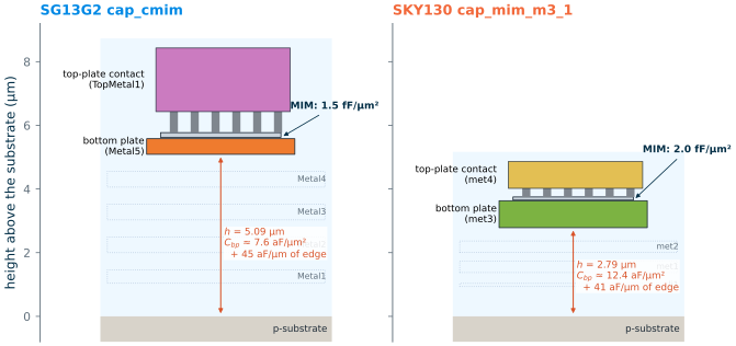
tools/3d/stacks.py, widths schematic). The bottom-plate coefficients are the area term of Eq. (26.3) at the plate height and the edge term discussed in the text.The bottom-plate capacitance \(C_{bp}\) is a plate capacitor of its own, with the whole back end below as its dielectric, plus a fringe along its edges:
\[C_{bp} \approx \frac{\varepsilon_{ox}}{h}\,A_{bp} + c_e P_{bp}, \tag{26.3}\]where \(h\) is the height of the bottom plate above the substrate, \(A_{bp}\) and \(P_{bp}\) its area and perimeter, and \(c_e\) the fringe capacitance per unit length of edge. For the oxide stack, SG13G2’s own Metal1-to-substrate value (37 aF/µm² at 1.04 µm) implies an effective \(\varepsilon_r\) of 4.35; at the 5.09 µm of Metal5 this gives 7.6 aF/µm². Magic’s SKY130 rules use 12.37 aF/µm² for met3 at 2.79 µm [15, 20]. The fringe term depends only logarithmically on the height, and two independent sources agree on its size: Magic uses 41 aF/µm for a met3 edge, and IHP’s RF model of the MIM capacitor, cap_rfcmim, contains 48 aF/µm of perimeter in its oxide capacitance [14]. We use 45 aF/µm for SG13G2.
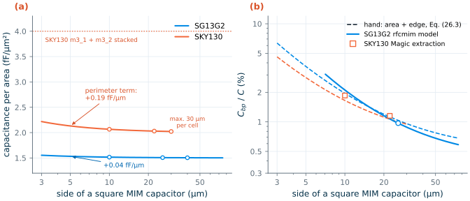
cap_rfcmim model (solid, valid from 7 µm) and Magic's full parasitic extraction of the SKY130 layouts (squares).Worked example 26.1 · A 1 pF MIM capacitor and its bottom plate, by hand and from the layouts
Size. With Eq. (26.2) for a square of side \(a\): SG13G2 needs \(1.5a^2 + 0.16a\) = 1000 fF, so \(a\) = 25.77 µm. Asked for C = 1 pF, the
cmimPyCell draws a MIM plate of exactly 25.76 µm, and the model gives 0.9995 pF. SKY130 needs \(2.0(a - 0.025)^2 + 0.76(a - 0.025)\) = 1000 fF, so \(a\) = 22.20 µm; the model of Magic’s 22.2 µm cell gives 1.000 pF. (These are the sides Chapter 15 used for the OTA’s Miller capacitor.)Bottom plate, SG13G2. The PyCell’s Metal5 plate encloses the MIM by 0.6 µm on every side (rule MIM.c), so it is 26.96 µm square: \(A_{bp}\) = 727 µm², \(P_{bp}\) = 107.8 µm. Eq. (26.3): 7.6 aF/µm² × 727 µm² + 45 aF/µm × 107.8 µm = 5.5 + 4.9 = 10.4 fF, 1.04 % of C. IHP’s
cap_rfcmimmodel of the same capacitor contains 9.7 fF between its plates and the substrate (simulated with both plates driven).Bottom plate, SKY130. Magic’s met3 plate is 24.36 × 22.60 µm, larger than the capm on the side where met4 drops down to contact it: \(A_{bp}\) = 551 µm², \(P_{bp}\) = 93.9 µm. Eq. (26.3): 12.37 × 551 + 40.99 × 93.9 aF = 6.8 + 3.8 = 10.7 fF, 1.07 %. Magic’s full extraction of the layout returns 11.5 fF from the bottom-plate terminal to the substrate, and 2.3 fF from the top plate (the edges of the met4 contact plate).
Result. By hand within 7 % of the PDK’s own numbers in both processes. In both, the bottom plate of a 1 pF MIM capacitor carries about 10 fF, 1 % of the capacitor; the top plate carries a fifth of that or less. For smaller capacitors the edge term grows in relative terms (Figure 26.3b): 1.9 % for a 10 µm SKY130 cell.
Layout rules that follow
- Put the bottom plate on the low-impedance node (Chapter 15). One per cent of the capacitor from a high-impedance node to a noisy substrate is a coupling path of 10 fF per picofarad; on a node driven by an amplifier output or a supply, it costs only a little extra load. In a switched-capacitor circuit the bottom plates face the input switches and the top plates the summing node, which is also what bottom-plate sampling needs (Chapter 19).
- Do not route under the bottom plate, and route over the top plate only with care. A wire in Metal4 under an SG13G2 MIM couples to the bottom plate at 68 aF/µm², nine times the substrate value. A wire in TopMetal2 over the TopMetal1 contact plate couples at 13 aF/µm² to the top plate, the sensitive one [15]. Most designs keep the area above and below a precision capacitor empty.
- Shield the bottom plate if the substrate is noisy. A grounded Metal4 (SG13G2) or met2 (SKY130) plate under the capacitor turns the 1 % to an unknown, noisy substrate into a larger but defined capacitance to a quiet ground: about 5 % of C in SG13G2 (68 aF/µm² over the Metal5 plate). That is a good trade for a sampling capacitor near digital circuits, a poor one where the bottom plate’s load matters.
- Keep the via array the generator draws. The thin top plate has a sheet resistance of 5.8 Ω/□ in SKY130 [18]; the generators contact it over its whole area so that the series resistance stays in the milliohms (55 mΩ in the SG13G2 model) and the capacitor keeps its quality factor up to radio frequencies.
Common pitfall · Extracting a SKY130 MIM capacitor twice
Magic’s full parasitic extraction of the 1 pF
cap_mim_m3_1returns, besides the device itself and the 11.5 fF of bottom plate, an extra 43 fF directly between the two plates (9.3 fF for a 10 × 10 µm cell): about 88 aF/µm², which is the met4-to-met3 overlap capacitance of the technology file applied across the whole capacitor. Physically, the capm plate lies between met4 and met3 and is on the met4 net, so that field is the MIM capacitor itself, already in the device model. The technology file places the MIM planes out of the usual shielding order, with a comment that this was done on purpose and “may want to reconsider” [20]. A post-layout simulation that keeps this element sees every MIM capacitor 4 to 5 % too large. Inspect the extracted netlist around MIM devices, and remove or discount the plate-to-plate term.
26.3 Metal-oxide-metal (fringe) capacitors
When a process shrinks, its metal lines get closer together faster than its layers get thinner. Two adjacent fingers of thickness \(t\) at a spacing \(s\) form a vertical plate capacitor of height \(t\), and a comb with a pitch \(p\) (finger plus gap) packs one such gap into every pitch. Per layer and per unit area, the lateral field alone gives about
\[\frac{C}{A} \approx \frac{\varepsilon_{ox}\,t}{s\,p}, \tag{26.4}\]and fringing between the finger tops and bottoms and between layers adds to it. At SG13G2’s minimum Metal2–Metal5 width and space (0.20 and 0.21 µm) and thickness (0.49 µm), Eq. (26.4) gives 0.21 fF/µm² per layer; SKY130’s met1 and met2 (0.14/0.14 µm, 0.36 µm thick) give 0.33 fF/µm² [16, 20]. Stacking combs in every metal layer and joining them with vias multiplies this, which is how a MOM capacitor approaches a MIM capacitor without an extra mask. Aparicio and Hajimiri showed that lateral-flux structures always win over plates once the line spacing falls below the layer spacing, and worked out how far [128].
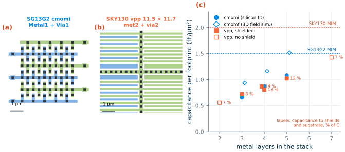
cap_cmomi (characterized on silicon) and cap_cmomf (from a 3D field simulation only), both 10 × 10 µm. SKY130: the fixed cap_vpp cells, labelled with the capacitance from both electrodes to the shields and the substrate, in per cent of the capacitance.Figure 26.4 puts numbers on it. SG13G2’s interdigitated cap_cmomi gains 0.27 fF/µm² of active area for each metal layer, 1.36 fF/µm² for all five, or 1.08 fF/µm² over the footprint including its feed bars; Eq. (26.4) accounts for about 80 % of each layer’s share. The fringe cell cap_cmomf, whose fingers change direction from layer to layer, is denser (1.52 fF/µm²), but its model comes from a field simulation, not from silicon. SKY130’s fixed cap_vpp cells range from 0.55 fF/µm² (met1 and met2 only) to 1.42 fF/µm² for the large cell that uses poly and all five metals [19, 18].
The price is in the parasitics. Both electrodes of a MOM capacitor are made of every layer, so both reach down to the substrate, and there is no “good plate” as in a MIM capacitor. The SKY130 models give each cell a capacitance from each electrode to the substrate and, for the shielded cells, to an li1 or poly plate below and a met5 plate above. From three simulations of each cell (one electrode driven, the other driven, both driven) we separate them: 7 to 14 % of the capacitance goes to shields and substrate, about ten times the MIM bottom plate, and the two electrodes are not equal (5.4 against 3.9 fF to the met5 shield of the 117 fF cell). The shields do not remove this capacitance; they make it a capacitance to a node you choose, usually a quiet ground, instead of to the substrate.
MOM capacitors have other strengths. They are linear, because metal does not deplete and the oxide is a good dielectric; they match very well, because their value is set by lithography over many fingers (Chapter 27); and they can be placed at any level, under a MIM capacitor, or inside a cell where a MIM would not fit. Their weak points in these open PDKs are documentation: SG13G2’s MOM models carry no corners, no mismatch and no temperature or voltage dependence, and the SKY130 cells are fixed sizes with a documented spread of about ±22 % (for example 74.6 fF, 57.8 to 91.4 fF, for the met1/met2 cell) [14, 18]. Hastings’s “woven” structures, in which vias tie the layers together throughout the array, also lower the series inductance [61]; both PDKs’ cells already tie their layers together with vias spread over the whole array.
The SG13G2 cmomi cell (5 × 5 µm, Metal1 to Metal5) and the SKY130 shielded vpp cell as 3D models. Hide the upper metals of the SG13G2 cell to see that every layer carries the same combs, joined by vias at the teeth; in the SKY130 cell, hide met5 and li1 to see the shields that sandwich the four finger layers.
IHP PyCell cmomi, w = l = 5 µm, mmin = 1, mmax = 5, double feed: 6.0 × 5.1 µm with feeds.
SkyWater's fixed cell as Magic places it: fingers in met1 to met4, shields in li1 and met5; 116.75 fF.
26.4 MOS capacitors and varactors
The C–V curve
A MOS capacitor is a transistor whose gate is one electrode and whose channel, source, drain and body together are the other. Its capacitance is the gate oxide’s \(C_{ox}\) in series with whatever capacitance the silicon beneath can offer:
\[\frac{1}{C} = \frac{1}{C_{ox}} + \frac{1}{C_{si}(V)}. \tag{26.5}\]For an NMOS structure in a p-type body, three regimes follow as the gate voltage rises [61]:
- Accumulation (gate well below the flat-band voltage): holes pile up at the surface, \(C_{si}\) is large, and \(C \approx C_{ox}\).
- Depletion (between flat band and threshold): the holes are pushed away and a depletion layer forms; \(C_{si}\) is the small capacitance of that layer, and \(C\) falls to a fraction of \(C_{ox}\).
- Inversion (above threshold): electrons from the source and drain form a channel at the surface, \(C_{si}\) becomes large again, and \(C\) returns to \(C_{ox}\). Without source and drain regions the electrons would have to be generated thermally, and the capacitance would stay low at any but the slowest signals; the diffusions are what make an inversion capacitor work at signal frequencies.
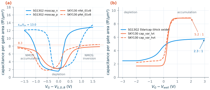
sg13_moscap_n/p, SKY130 nfet_01v8, pfet_01v8), 1 MHz, 27 °C. Dotted: \(\varepsilon_{ox}/t_{ox}\). (b) Accumulation-mode varactors in an n-well: SG13G2 sg13_hv_svaricap (thick oxide, Nx = 10 × 3.74 × 0.3 µm per gate) and SKY130 cap_var_lvt/hvt (5 × 0.5 µm).Figure 26.5a shows all three regimes in both PDKs. SG13G2’s moscap_n reaches 12.7 fF/µm² at 1.2 V, 97 % of \(\varepsilon_{ox}/t_{ox}\), and falls to 1.6 fF/µm² at 0 V; SKY130’s NMOS reaches 7.9 fF/µm² at 1.8 V and 2.2 fF/µm² at 0 V. In inversion or accumulation, a MOS capacitor is 8 times denser than SG13G2’s MIM and 4 times denser than SKY130’s, but only there. The PMOS curves are the mirror image: inversion for negative gate voltages, accumulation of the n-well’s electrons for positive ones.
Which terminal goes where
The gate is the “good” electrode: a poly plate on oxide, like the top plate of a MIM. The other electrode is silicon, and it carries junction capacitance and leakage to everything around it: the source and drain junctions to the body, and for a PMOS the n-well’s junction to the substrate. Hence the choice [61]:
- A capacitor to ground (decoupling, a loop filter, a node capacitance): an NMOS in inversion with source, drain and body on ground, gate on the node, which must sit above threshold. All its junctions are then shorted.
- A capacitor to the supply: a PMOS in inversion with source, drain and n-well on \(V_{DD}\), gate on the node, which must sit well below \(V_{DD}\).
- A capacitor between two signal nodes: an accumulation structure in an n-well (a varactor used at one end of its range), with the well on the node of lower impedance, since the well’s junction to the substrate hangs on it.
The silicon electrode is also resistive. The channel of an inversion capacitor is a sheet of a few kilohms per square, contacted only at its source and drain edges, so a long gate is a distributed RC line like the resistors of Chapter 25. For decoupling at high frequency, use many short fingers (L of a few micrometres), not one large square.
Varactors
The varactors of both PDKs are accumulation-mode devices: a gate over an n-well contacted by n+ diffusions, so there are no holes to form an inversion layer, and the capacitance moves smoothly from depletion (gate negative relative to the well) to accumulation (gate positive). Figure 26.5b compares them. SKY130’s cap_var_lvt, on the 4.15 nm core oxide, tunes 5.2 : 1 (1.7 to 8.9 fF/µm² of gate) within half a volt around zero; cap_var_hvt 4.0 : 1 [19]. SG13G2’s SVaricap uses the 7 nm thick oxide and tunes only 2.3 : 1 (2.5 to 5.8 fF/µm²), but over ±3 V, which suits an LC oscillator whose swing is large. Its specification lists 23 to 39.5 fF/µm² at −3 and +3 V, measured at 15.8 GHz on a ten-cell test structure [15]; that normalization cannot be per gate area, since the oxide alone allows only 4.9 fF/µm², so compare the PDKs through the model and the tuning ratio. Varactor design itself, with its quality factor and tuning range, belongs to RF and oscillator texts; Chapter 22 used a ring oscillator instead.
Worked example 26.2 · A MOS capacitor for the PLL loop filter
The charge-pump PLL of Chapter 22 needs a loop-filter capacitor \(C_1\) of 63.8 pF in SG13G2 and 46.4 pF in SKY130, from the control node to ground, with the control voltage in lock at 0.64 V and 1.03 V. As MIM, that is 42 500 µm² in SG13G2 (a quarter of the recommended MIM area per chip) and 23 200 µm² in SKY130 (11 600 µm² stacked).
Area as an NMOS inversion capacitor. At 0.64 V the SG13G2
moscap_ngives 11.9 fF/µm² (Figure 26.5a): 63.8 pF needs 5370 µm², 7.9 times less than MIM. At 1.03 V SKY130’s NMOS gives 7.6 fF/µm²: 6100 µm², 3.8 times less than one MIM layer.Does the value hold? Over the SG13G2 tuning range (0.35 to 1.2 V) the capacitance per area moves from 10.2 to 12.7 fF/µm², −14 % to +7 % around the lock point. In a loop filter that only shifts the zero \(1/(RC_1)\) and the phase margin by a few degrees (Chapter 22), which is why MOS capacitors are acceptable here and not in a switched-capacitor filter.
Leakage. The SG13G2 model includes gate tunnelling through the 2.65 nm oxide: 14 pA/µm² at 0.64 V, so 5370 µm² leak 77 nA. The charge pump must replace that current every cycle, so the loop settles with a static phase offset of \(2\pi I_{leak}/I_{CP}\) = 2π × 77 nA/20 µA = 0.024 rad (1.4°) and a reference spur from the correction pulses. At the top of the tuning range (1.2 V) the leakage is 400 pA/µm², 2.1 µA in total, a tenth of the charge-pump current. The SKY130 models contain no gate current at all, so simulation cannot answer the question there; direct tunnelling falls roughly exponentially with oxide thickness, so SKY130’s 4.15 nm oxide leaks orders of magnitude less than SG13G2’s 2.65 nm one.
Result. A MOS loop-filter capacitor saves 75 to 90 % of the area in both PDKs. In SG13G2, check the leakage at the highest control voltage, or use a thick-oxide device (the
SVaricapin accumulation gives 5.8 fF/µm² with negligible leakage, still four times the MIM density).
Common pitfall · A MOS capacitor that is not biased where you think
A MOS capacitor drawn as “a big gate” and connected without thought may sit in its depletion dip: at 0 V an SG13G2 NMOS capacitor has 1.6 fF/µm², an eighth of its nominal value, and a circuit that relies on 12.7 fF/µm² will miss its bandwidth or its phase margin by that factor. Every MOS capacitor needs a DC operating point at least 0.5 V beyond threshold or flat band over all corners and temperatures, and a check in simulation at the extremes of its voltage. Decoupling capacitors from the core supply to ground meet this automatically; capacitors on signal nodes often do not.
26.5 Voltage and temperature coefficients
The PDKs describe the drift of a capacitor with polynomial coefficients around a reference voltage and temperature:
\[C(V) = C_0\left[1 + VC_1\,V + VC_2\,V^2\right], \qquad C(T) = C(T_0)\left[1 + TC_1\,(T - T_0) + TC_2\,(T - T_0)^2\right]. \tag{26.6}\]A voltage coefficient turns into distortion. A capacitor whose value depends on its voltage stores the charge \(Q = C_0\,(V + VC_1V^2/2 + VC_2V^3/3)\); driven with \(V = A\sin\omega t\), the second term produces a second harmonic of relative size
\[HD_2 = \frac{VC_1\,A}{4}, \qquad HD_3 = \frac{VC_2\,A^2}{12}. \tag{26.7}\]A fully differential circuit cancels the even term and leaves the odd one.
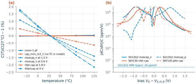
MIM capacitors. SG13G2 specifies \(VC_1\) = −26 ppm/V, \(VC_2\) = +5 ppm/V², \(TC_1\) = +3.6 ppm/K and \(TC_2\) = 0.002 ppm/K², measured from −10 to +10 V and from −40 to 125 °C [15]. The model carries the temperature coefficients (our simulation returns +3.7 ppm/K) but not the voltage ones. With a 0.5 V amplitude, Eq. (26.7) gives \(HD_2\) = 3.3 ppm (−110 dB) and \(HD_3\) = 0.1 ppm: far below anything else in a CMOS circuit. SKY130’s documents give no coefficients, and its model has none; the residual effects of a metal–nitride–metal stack are of the same order in any process, but the number is not published. Both are linear enough for any switched-capacitor circuit or data converter of this course.
MOM capacitors are, physically, as linear as MIM: metal electrodes and oxide. Their temperature coefficient comes mostly from the thermal expansion of the stack and the permittivity of the oxide, tens of ppm/K at most. Neither PDK’s model contains either coefficient.
MOS capacitors are a different class (Figure 26.6b). Even in strong inversion the capacitance still rises with voltage, because the charge layer moves closer to the oxide and the poly gate depletes less: 5.3 %/V for SG13G2 at 1.2 V and 2.5 %/V for SKY130 at 1.8 V, rising to 27 %/V at 0.6 V in SG13G2 and to 10⁶ ppm/V in the depletion dip. Eq. (26.7) with \(VC_1\) = 5.3 %/V and a 0.25 V amplitude gives \(HD_2\) = 0.33 % (−50 dB), 60 dB worse than the MIM capacitor. Their temperature coefficients at the core supply are −150 ppm/K (SG13G2) and −68 ppm/K (SKY130), and several thousand ppm/K in depletion, where the threshold voltage moves with temperature (Table 26.2).
Table 26.2. Voltage and temperature coefficients: specification values and fits to the simulations of Figures 26.5 and 26.6 (27 °C reference; linear TC from −40 to 125 °C) [15, 14, 19].
| Quantity | SG13G2 | SKY130 |
|---|---|---|
| MIM, voltage coefficient | −26 ppm/V, +5 ppm/V² (spec); none in model | not specified; none in model |
| MIM, temperature coefficient | +3.6 ppm/K (spec), +3.7 (model) | none in model |
| MOM | no coefficients in the models | no coefficients in the models |
| NMOS capacitor at \(V_{DD}\): \(\vert dC/dV\vert/C\) | 5.3 %/V (1.2 V) | 2.5 %/V (1.8 V) |
| NMOS capacitor at \(V_{DD}\): TC | −150 ppm/K | −68 ppm/K |
| NMOS capacitor at 0.6 V: \(\vert dC/dV\vert/C\), TC | 27 %/V, −204 ppm/K | (in depletion) |
| Varactor at 0 V: TC | −240 ppm/K (SVaricap) | none in model (lvt) |
| Gate leakage of a core NMOS capacitor at \(V_{DD}\) | 0.40 nA/µm² (1.2 V) | not modelled |
What this means for your design
Sort the capacitors of a design by what their value must do. Signal capacitors that set gain, filter poles or charge ratios, with a voltage that changes across them (switched-capacitor circuits, sample-and-holds, Miller capacitors, DAC arrays), must be MIM or MOM: their coefficients are parts per million. Tolerant capacitors whose value may move by 10 or 20 % (loop filters, decoupling, slow integrators of a bias loop) can be MOS, four to eight times smaller, provided the bias keeps them out of depletion and, in SG13G2’s thin oxide, the leakage is acceptable. Tuning capacitors are varactors. The density argument is only worth having for large capacitors: below a few picofarads, the routing and spacing around a capacitor cost more area than the capacitor itself.
26.6 On-chip inductors in brief
An inductor stores energy in the magnetic field of its current. On a chip it is a spiral of the thickest, highest metal: SG13G2 has a parametric PyCell (inductor2, inductor3) in its 3 µm TopMetal2, 11 µm above the substrate; SKY130 provides fixed test coils in its 0.845 µm met3, 2.8 µm above the substrate, and three inductor models (3D gallery). A few nanohenries are all a practical spiral offers, so inductors appear only where frequencies are in the gigahertz: LC oscillators, matching networks, peaking in wideband amplifiers. Three numbers describe one: the inductance \(L\), the series resistance \(R_s\) (and with it the quality factor \(Q\)), and the self-resonant frequency, above which the parasitic capacitance makes the device capacitive.
Inductance
The turns of a spiral couple to each other, so its inductance grows faster than linearly with the number of turns. Treating the turns as a uniform sheet of current, Mohan et al. derived a compact expression that is accurate to a few per cent for square and octagonal spirals [127]:
\[L = \frac{\mu_0 n^2 d_{avg} c_1}{2}\left[\ln\frac{c_2}{\rho} + c_3\rho + c_4\rho^2\right], \quad d_{avg} = \frac{d_{out} + d_{in}}{2}, \quad \rho = \frac{d_{out} - d_{in}}{d_{out} + d_{in}}, \tag{26.8}\]with \(n\) turns between the inner and outer diameters \(d_{in}\) and \(d_{out}\), and \((c_1, c_2, c_3, c_4)\) = (1.07, 2.29, 0, 0.19) for an octagon. The fill ratio \(\rho\) says how much of the spiral is metal; inner turns of a well-filled spiral enclose little flux and add resistance more than inductance, so good spirals are hollow (\(\rho\) ≈ 0.2 to 0.4). A second, independent estimate sums the partial inductances of the straight segments: the self-inductance of each bar plus the mutual inductance of every pair, computed with Neumann’s double integral over their centre lines [64]. fig_ind() in tools/figs/ch26_capacitors.py does both, from the geometry read off the generated layouts.
Resistance, quality factor and self-resonance
The DC resistance is the sheet resistance times the number of squares of the track: 11 mΩ/□ for SG13G2’s TopMetal2, 47 mΩ/□ for SKY130’s met3 [15, 19]. At high frequency the current crowds into a skin of depth
\[\delta = \sqrt{\frac{\rho_m}{\pi f \mu_0}}, \qquad R_s(f) \approx R_{DC}\,\frac{x}{1 - e^{-x}}, \quad x = \frac{t}{2\delta}, \tag{26.9}\]on the top and bottom faces of a track of thickness \(t\) and resistivity \(\rho_m\); in aluminium at 5 GHz, \(\delta\) ≈ 1.3 µm, less than half of TopMetal2’s 3 µm. Currents induced in neighbouring turns crowd it further (the proximity effect), and currents induced in the substrate below add a loss that grows with frequency. The quality factor
\[Q = \frac{\mathrm{Im}\,Z}{\mathrm{Re}\,Z} \approx \frac{\omega L}{R_s} \tag{26.10}\]rises with frequency until these losses and the capacitance of the spiral to the substrate (the oxide capacitance \(C_{ox} = \varepsilon_{ox}A/h\) under the track area \(A\)) turn it over; at the self-resonant frequency the inductance and \(C_{ox}\) resonate and \(Q\) falls to zero.
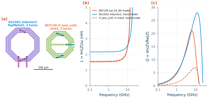
inductor2 (3 turns, w = 8 µm, s = 2.1 µm, din = 124 µm) and SkyWater's fixed rf_test_coil1 (3 turns, w = 7.5 µm, s = 2.5 µm, din = 90 µm), same scale. (b, c) Inductance and quality factor, one port driven, the other grounded: SKY130's ind_03_90 model, and hand models from the layouts (L from the partial-inductance sum, R from the sheet resistance with Eq. (26.9), half of \(C_{ox}\) at the port; substrate eddy-current loss neglected).Worked example 26.3 · A spiral inductor from its layout, in both PDKs
SG13G2,
inductor2with 3 turns, w = 8 µm, s = 2.1 µm (Figure 26.7a). The smallest inner diameter the PyCell accepts for three turns of this width is 123.9 µm; we draw 124 µm, and the TopMetal2 outline is 180.4 µm across, so \(d_{avg}\) = 152.2 µm and \(\rho\) = 0.185. Eq. (26.8): \(L\) = (4π × 10⁻⁷ × 9 × 152.2 µm × 1.07/2) × [ln(2.29/0.185) + 0.19 × 0.185²] = 0.921 nH × 2.52 = 2.32 nH. The partial-inductance sum over the centre lines, with the real 3 µm thickness, gives 2.15 nH: thick tracks have slightly less inductance than the thin current sheet of Eq. (26.8). The centre lines of the three octagons are 1513 µm long, 189 squares of 8 µm: \(R_{DC}\) = 189 × 11 mΩ = 2.08 Ω. At 5 GHz, Eq. (26.9) with \(\rho_m\) = 11 mΩ × 3 µm gives δ = 1.29 µm and \(R_s\) = 1.69 × 2.08 = 3.52 Ω, so \(Q\) = 2π × 5 GHz × 2.15 nH/3.52 Ω = 19 (18.5 once the oxide capacitance below is included). The track covers 11 650 µm² at 11.2 µm above the substrate: \(C_{ox}\) = 4.1ε₀ × 11 650 µm²/11.2 µm = 38 fF, and with half of it at the driven port the spiral resonates at about 25 GHz. As a check of Eq. (26.8) on IHP’s own numbers: the PyCells’ built-in estimates for their default geometries are 33.3 pH (inductor2, one turn, d = 15.48 µm) and 221.5 pH (inductor3, two turns), against 35.2 and 214 pH from Eq. (26.8), +6 % and −3 % [14].SKY130,
rf_test_coil1(Figure 26.7a): 3 turns of 7.5 µm with 2.5 µm spaces, 145.0 µm outside, so \(d_{in}\) = 145.0 − 6 × 7.5 − 4 × 2.5 = 90.0 µm. Eq. (26.8): 1.63 nH; partial-inductance sum: 1.56 nH. That geometry, three turns around a 90 µm opening with a centre tap, is what the name of SkyWater’s modelind_03_90describes, and the model’s inductance is 1.53 nH at 1 GHz, within 2 % of the sum. Its resistance is another matter: the coil’s centre lines are 1168 µm of met3, 156 squares at 47 mΩ/□, \(R_{DC}\) = 7.3 Ω, while the model has 2.06 Ω. At 5 GHz, the met3 coil has \(Q\) ≈ 5; the model claims 20 (Figure 26.7c). The self-resonant frequencies agree (16.5 GHz by hand, 16.9 GHz in the model), so the model’s capacitances fit this geometry; only its losses do not fit a met3 coil. They would fit a coil strapped in met3, met4 and met5: the three sheets in parallel give 12.9 mΩ/□ and 2.0 Ω for the same 156 squares.Result. Eq. (26.8) is within 8 % of the partial-inductance sum and of the PDK numbers in both processes, which is as good as a hand estimate needs to be; the series resistance and the substrate decide \(Q\), and they must come from an electromagnetic simulation or a measurement.
SG13G2 vs SKY130 · Inductors
SG13G2 is an RF process: two thick top metals far above a 50 Ω·cm substrate [15], a parametric inductor PyCell that also paints no-fill markers on every layer, a p-well block and a no-extraction marker over its whole footprint, and an EM-simulation flow documented with the PDK. For the same geometry, its TopMetal2 has a quarter of the sheet resistance of SKY130’s met3 and sits four times higher, and our estimates give it four times the \(Q\) (Figure 26.7c). SKY130 ships three fixed test coils and three inductor models whose layouts are not identified in the open documents; the one whose name matches
rf_test_coil1has a third of the resistance that coil’s met3 can have. Use SKY130 inductors only with your own EM simulation, or strap met3, met4 and met5 in parallel, which brings the resistance to the model’s value (Worked example 26.3).
Layout rules for inductors
Most of the physics of this section turns into a handful of rules [61]:
- Use the thickest, highest metal for the spiral and a lower one only for the crossings and the underpass. Resistance falls with thickness, and the capacitance to the substrate falls with height. In SKY130, where no thick metal exists, straps of met3 to met5 in parallel are the closest substitute.
- Keep the spiral hollow and the track moderately wide. Inner turns add resistance and little inductance; very wide tracks add capacitance and, at high frequency, carry current only on their edges.
- Keep metal, fill and other circuits out of the inductor’s field. Eddy currents in any closed metal loop nearby cost \(Q\) and change \(L\); the SG13G2 PyCell’s no-fill markers exist for this. Leave a clearance of the order of the inductor’s diameter to sensitive circuits, and do not route lines through or over it.
- Mind the substrate. A patterned ground shield, a grounded poly or low-metal grid under the spiral whose fingers are cut perpendicular to the induced currents so that no eddy loop can form, terminates the electric field before it reaches the lossy substrate without short-circuiting the magnetic one; Yue and Wong measured clearly higher \(Q\) with it [126]. Substrate contacts around (not under) the inductor keep its substrate potential defined.
Try it · Resize a capacitor, reshape an inductor
In
tools/layout/ch26/gen_cap_sg13g2.py, changecmim_1ptoC="0.2p"and rerunpython3 tools/layout/ch26/cap_layouts.py: read the new plate size fromtools/layout/ch26/shapes.json, compute the bottom-plate capacitance with Eq. (26.3), and compare its fraction with the 1 pF case and withrfcmim_cox()intools/figs/ch26_capacitors.py. Then changeinductor2_n3to two turns of 12 µm width and runpython3 tools/figs/ch26_capacitors.py indafter updatinggeo["sg13g2"]infig_ind()with the new dimensions: does \(L\) fall as \(n^2\), and does the wider track raise \(Q\) at 5 GHz as much as you expected from Eq. (26.9)?
- MIM capacitors give 1.5 fF/µm² (SG13G2) and 2.0 fF/µm² (SKY130, 4.0 stacked) with coefficients of parts per million: −26 ppm/V and +3.6 ppm/K in SG13G2. Their bottom plate carries about 1 % of the capacitance to the substrate at 1 pF; Eq. (26.3) predicts it within 7 % of the PDK models and extraction. Put it on the low-impedance node.
- MOM capacitors need no extra mask and reach 1.08 to 1.52 fF/µm² in five SG13G2 metals and up to 1.42 fF/µm² in SKY130’s cells, but couple 7 to 14 % of their value to shields and substrate, and their models in both PDKs carry no corners or coefficients.
- MOS capacitors are 4 to 8 times denser than MIM (12.7 and 7.9 fF/µm² at the core supply) but only away from their depletion dip, with voltage coefficients of 2.5 to 5 %/V and, in SG13G2’s 2.65 nm oxide, a leakage of 0.4 nA/µm² at 1.2 V. Use them where 10 to 20 % does not matter: decoupling and loop filters.
- Varactors tune 5.2 : 1 (SKY130
cap_var_lvt, ±2 V) and 2.3 : 1 (SG13G2 thick-oxideSVaricap, ±3 V).- Magic’s full extraction double-counts about 4.5 % of plate-to-plate capacitance in SKY130 MIM capacitors; inspect extracted netlists around capacitors.
- A spiral’s inductance follows Eq. (26.8) within 8 %; its \(Q\) follows the metal: about 18 at 5 GHz for a 2.2 nH SG13G2 TopMetal2 spiral, about 5 for a 1.6 nH SKY130 met3 coil, whose PDK model claims 20.
Further reading
- R. A. Hastings, The Art of Analog Layout [61], Chapter 7: the full range of integrated capacitors, from junction and poly–poly capacitors to trench and lateral-flux structures, their variability and parasitics, and planar inductors with their loss mechanisms.
- IHP, SG13G2 Process Specification [15], sections 2.11, 2.12, 2.16 and 2.17 (varicap, MIM, layer thicknesses, parasitic capacitances), and the model files
capacitors_mod.lib,cap_cmomi.libandcap_cmomf.libof the PDK [14], whose headers say plainly what each model does and does not contain. - The SkyWater device documentation [18] for the MIM, VPP and varactor test data, and the SKY130 model files [19] for the
cap_vppcells and inductors. - R. Aparicio and A. Hajimiri [128]: why lateral-flux capacitors win as processes shrink, and how to draw them.
- S. S. Mohan et al. [127] for the inductance expressions of Eq. (26.8), and C. P. Yue and S. S. Wong [126] for the spiral’s equivalent circuit and the patterned ground shield.