Chapter 23
Layout Fundamentals: From Masks to Rules
A layout is a set of masks. Knowing what each drawn layer becomes in SG13G2 and SKY130, and why every design rule exists, is the base of all analog layout craft. This chapter follows one transistor from polygons to silicon, reads the rule decks of both PDKs, and then draws the transistor by hand until the decks are satisfied.
- Explain how drawn layers become masks, implants, films and devices, and draw the cross-section of a transistor from its layout.
- Read the layer sets of SG13G2 and SKY130, map one onto the other, and explain the derived layers a rule deck computes.
- Explain the physical reason behind width, spacing, enclosure, extension, density, antenna and latch-up rules, and find their values in the PDK files.
- Run each PDK’s DRC from the command line and read its report.
- Draw a transistor by hand in both PDKs, make it pass DRC and LVS, and compare it with the PDK’s generator.
Contents
- 23.1 From masks to devices: what each drawn layer makes
- 23.2 The layer sets of SG13G2 and SKY130
- 23.3 Design rules and why they exist
- 23.4 Density, antenna and other chip-level rules
- 23.5 Working in KLayout and Magic: grids, hierarchy, PCells and DRC
- 23.6 Drawing a transistor by hand
- 23.7 Layout as communication: names, labels, pins and notes
- Further reading
Chapter 15 used the PDKs’ device generators and treated the layers and rules as given; Chapter 16 ran the checks; Chapter 17 described the process steps. This chapter sits underneath all three. It asks what a drawn polygon is, where each rule comes from, and what is left for you to decide once the rules are met. Everything here is computed from the PDK files and checked with the PDKs’ own decks, in IIC-OSIC-TOOLS [35].
23.1 From masks to devices: what each drawn layer makes
A drawn layer is a set of polygons in the layout database with a layer number and a datatype (also called its purpose): Activ 1/0 in SG13G2, diff 65/20 in SKY130. A mask is a quartz plate with a chromium pattern that exposes photoresist on the wafer in one lithography step. The two are related but not the same. The foundry turns the drawn layers into masks with Boolean operations, size adjustments and optical proximity correction (OPC), and some masks have no drawn layer of their own [61].
SG13G2 shows this openly in its layer table [16]:
- The n+ implant mask is computed, not drawn. The rules define it as nSD = NOT(pSD OR nSD:block): every region that is not marked p+ receives the n+ source/drain implant. You never draw an n+ layer for an NMOS in SG13G2; the drawn nSD layer exists only for the rare devices that need both implants, such as the
rhighresistor. - Some layers have a mask datatype (Activ 1/20, Metal1 8/20, …) that is “added to the drawing at mask generation”, and the lithography-critical layers have OPC datatypes (Activ 1/26 and 1/27, GatPoly 5/26 and 5/27, Cont 6/26, Metal1 8/26, …). These belong to the foundry. That list is a map of which of your layers are printed close to the resolution limit.
SKY130 needs both implants drawn (nsdm for n+, psdm for p+), and its layer properties list a second family of names starting with c (cfom, cp1m, cli1m, cmm1, …): the mask layers that SkyWater generates from the drawn ones [18]. You draw the layers without the c.
What each layer does to the wafer
Table 23.1 follows the front-end masks of an NMOS and a PMOS in the order the process uses them. Chapter 17 describes the process steps themselves; here the point is the link between a polygon you draw and a feature on the wafer.
Table 23.1. From drawn layer to wafer (front end and first metal) [16, 18, 63].
| Drawn layer (SG13G2 / SKY130) | What the mask does | What you get on the wafer |
|---|---|---|
| Activ / diff, tap | Protects silicon from the trench etch (an inverted mask) | Silicon inside the shape; trench oxide (STI) everywhere outside it |
| NWell / nwell | Opens the resist for the n-well implant | An n-type well for PMOS devices and n-well resistors |
| ThickGateOx / hvi | Marks where the thick oxide stays | 3.3 V (SG13G2) or 5 V (SKY130) gate oxide |
| GatPoly / poly | Patterns the polysilicon film | Gates where it crosses active area, poly wires elsewhere |
| (NOT pSD) / nsdm | Opens the resist for the heavy n-type implant | n+ source and drain, n-well ties |
| pSD / psdm | Opens the resist for the heavy p-type implant | p+ source and drain, substrate ties |
| SalBlock / rpm, urpm | Blocks the silicide reaction | Unsilicided poly or active: precision resistors |
| Cont / licon | Etches holes through the pre-metal oxide | Tungsten plugs down to active or poly |
| — / li1, mcon | Patterns a thin film, then a second contact | Local interconnect and its contacts to met1 (SKY130 only) |
| Metal1 / met1 | Patterns the first aluminium film | First-level wiring |
Two consequences shape every rule in Section 23.3.
- The transistor is self-aligned. The source/drain implant mask is much larger than the transistor; the poly gate itself shields the channel from the implant, so the channel length is set by the poly etch alone. That is why the implant layers have loose rules (a pSD shape must be at least 0.31 µm wide) while the gate has the tightest rule of the process.
- Active area is defined by what you do not draw. Wherever there is no Activ or diff, the silicon is etched away and filled with oxide. The trench between two active shapes is a device too: a field transistor whose gate is any wire passing above. The spacing rules keep it off.
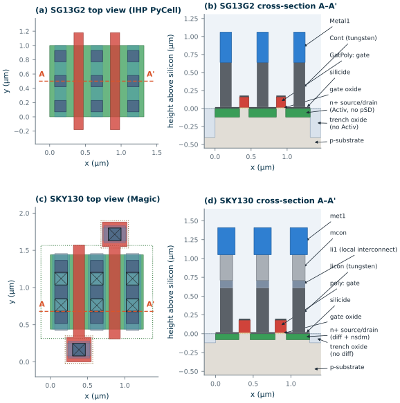
tools/figs/ch23_fundamentals.py from the GDS polygons and the layer heights of tools/3d/stacks.py (SG13G2 process specification; SKY130 stack as in Magic's technology file), at the same scale in x and z. Above the silicon everything is to scale; below it the drawing is schematic (junction depth, and a trench depth of 0.4 µm in SG13G2 and 0.12 µm as in Magic's SKY130 stack). Metal1 ends 1.06 µm above the silicon in SG13G2, met1 1.41 µm in SKY130.Read Figure 23.1 from the bottom up. The trench oxide appears exactly where the top view has no green; the n+ regions sit between the gates and the trench; the gates are the parts of the red poly that cross the active area; each dark contact column becomes a tungsten plug. SG13G2’s 0.64 µm tall contacts land directly on Metal1. SKY130 stacks three layers for the same job: a licon plug ending 0.61 µm above the silicon, 0.10 µm of li1, and an mcon of 0.34 µm up to met1. The cut through the SKY130 cell is at y = 0.68 µm, one of the two heights where a licon and an mcon overlap: Magic staggers the two contact arrays, which does not matter electrically, because li1 connects them.
Try it · Cut your own cross-section
fig_masks()intools/figs/ch23_fundamentals.pycuts any GDS along a horizontal line. Point it attools/3d/gds/sky130_pmos.gds(the PMOS of the 3D gallery) and add the n-well to the slabs: the p+ regions now sit in an n-type well, and the guard ring shows up as two extra active regions at the ends of the cut.
23.2 The layer sets of SG13G2 and SKY130
Each PDK defines well over a hundred layer/datatype pairs; an analog designer draws about twenty-five. Table 23.2 maps them onto each other, with the GDS numbers read from the SG13G2 layer table and the SKY130 KLayout layer properties and rule deck. Table 15.1 gave the first dozen; this is the full working set.
Table 23.2. The drawn layers of the two PDKs, as layer/datatype [16, 18, 20].
| Function | SG13G2 | SKY130 |
|---|---|---|
| Active area of transistors and diodes | Activ 1/0 | diff 65/20 |
| Substrate and well ties | Activ 1/0 (p+ with pSD) | tap 65/44 |
| n-well; deep n-well | NWell 31/0; nBuLay 32/0 | nwell 64/20; dnwell 64/18 |
| n+ implant | not drawn: NOT(pSD OR nSD:block) | nsdm 93/44 |
| p+ implant | pSD 14/0 | psdm 94/20 |
| Threshold-voltage implants | — | lvtn 125/44, hvtp 78/44 |
| Thick gate oxide | ThickGateOx 44/0 | hvi 75/20 |
| Gate and poly wiring | GatPoly 5/0 | poly 66/20 |
| Resistor and salicide-block layers | SalBlock 28/0, PolyRes 128/0 | poly.res 66/13, rpm 86/20, urpm 79/20 |
| Nitride cut around poly contacts | — | npc 95/20 |
| Contact to active and poly | Cont 6/0 | licon 66/44 |
| Local interconnect; its contact to met1 | — | li1 67/20; mcon 67/44 |
| Metal1; Via1 | Metal1 8/0; Via1 19/0 | met1 68/20; via 68/44 |
| Metal2 to Metal5 | 10/0, 30/0, 50/0, 67/0 | met2 to met5 69/20 … 72/20 |
| Via2 to Via4 | 29/0, 49/0, 66/0 | via2 to via4 69/44 … 71/44 |
| Thick top metals and vias | TopVia1 125/0, TopMetal1 126/0, TopVia2 133/0, TopMetal2 134/0 | — |
| MIM top plate; its via | MIM 36/0 (above Metal5); Vmim 129/0 | capm 89/44 (above met3), cap2m 97/44 (above met4) |
| Pad opening | Passiv 9/0 | pad 76/20 |
| Pin shapes (connectivity only) | datatype 2, e.g. Metal1 8/2 | datatype 16, e.g. met1 68/16 |
| Net labels (text) | datatype 25, e.g. Metal1 8/25; TEXT 63/0 for notes | datatype 5, e.g. met1 68/5; text 83/44 |
| Fill; fill exclusion | datatype 22; datatype 23 | generated by the fill script (Chapter 17) |
| Cell outline | prBoundary 189/0 | prBoundary 235/4 |
Most rows map one to one. Three do not.
SKY130’s local interconnect has no SG13G2 equivalent. In SG13G2 a contact (Cont) is a tungsten plug from the silicon to Metal1. In SKY130 the same job takes three layers: licon from the silicon to li1, a 0.1 µm film of titanium nitride, and mcon from li1 to met1 [18]. li1 comes from the process’s dense digital cells, where it wires transistors together underneath met1 and saves a metal layer. For analog work it is a short-distance layer: at 12.8 Ω/□ it is a hundred times more resistive than met1 (Chapter 15). When you move a layout from one PDK to the other, an SG13G2 Cont becomes a licon–li1–mcon stack, each with its own width, spacing and enclosure rules, and the SKY130 li1 wiring must move up to Metal1 in SG13G2.
SG13G2 has no n+ layer to draw, SKY130 has no p-well. SG13G2 derives n+ from the absence of pSD; SKY130 asks for nsdm and psdm explicitly, and Magic generates them for you when it writes GDS (Section 23.5). Neither PDK has a drawn p-well: the NMOS devices sit in the p-substrate (or a p-well implant the foundry places wherever there is no n-well).
SG13G2’s back end is taller. Two thick top metals (2 and 3 µm) with their own vias have no SKY130 counterpart, and the MIM capacitor sits above Metal5 instead of above met3 (Chapter 3).
Purposes: drawing, pin, label, fill
The datatype says what a shape is for. Drawing shapes (SG13G2 datatype 0, SKY130 datatype 20 or 44) go to the masks. Pin shapes (2 and 16) mark where a net may be connected from outside the cell and labels (texts on 25 and 5) name the nets; neither is fabricated, but LVS and the place-and-route tools read them (Section 23.7). Fill shapes (SG13G2 22) are the dummy pieces added for density; nofill (23) shapes forbid them. Only the drawing purposes count for DRC of the device, which is why the IHP rules insist that every pin shape is fully covered by drawing (rules Pin.a to Pin.h) [16].
Derived layers: what the rule deck sees
A rule deck does not check your drawn layers directly. It first computes derived layers with Boolean operations (AND, OR, NOT, and sizing) that correspond to physical objects, and then measures those [61]. Table 23.3 lists the derivations that the SG13G2 deck (ihp-sg13g2.drc, section “common derivations”) makes for MOSFETs; Magic does the same for SKY130 when it reads a GDS file and turns diff, nsdm and poly into its device types.
Table 23.3. Derived layers for MOSFETs, as the decks compute them [16, 14, 40].
| Derived layer | SG13G2 deck | SKY130 (Magic types, KLayout deck) |
|---|---|---|
| p-well (where NMOS live) | pwell = chip NOT PWell:block NOT NWell | everything outside nwell |
| n+ active | nactiv = Activ NOT (pSD OR nSD:block) | (diff OR tap) AND nsdm |
| p+ active | pactiv = Activ AND pSD | (diff OR tap) AND psdm |
| substrate tie | ptap = pactiv AND pwell | tap AND psdm, outside nwell |
| n-well tie | ntap = nactiv AND NWell | tap AND nsdm, inside nwell |
| NMOS gate | ngate = (nactiv AND pwell) AND GatPoly | diff AND nsdm AND poly (Magic type nfet) |
| PMOS gate | pgate = (pactiv AND NWell) AND GatPoly | diff AND psdm AND poly in nwell (pfet) |
| contact kind | Cont on Activ; Cont on GatPoly | licon on diff (ndc, pdc); licon on poly (pc) |
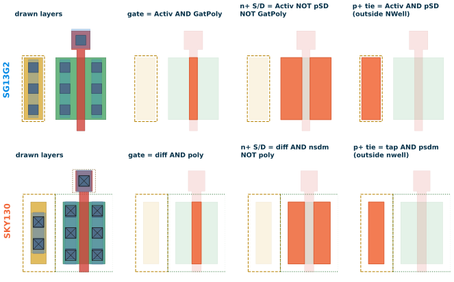
Figure 23.2 applies three of them to the transistor drawn in Section 23.6. Derived layers explain rules that would otherwise look arbitrary. SG13G2’s rule Gat.a1, minimum gate length of a 1.2 V NFET, is a width check on ngate NOT ThickGateOx, not on the poly; its LU.b, the latch-up rule, grows every ptap by 20 µm (in 0.5 µm steps, so that the growth follows the substrate around obstacles) and reports whatever nactiv AND pwell is left uncovered. Once you know the derivation, a violation marker tells you which physical object is wrong.
23.3 Design rules and why they exist
A design rule is a geometric limit that keeps the fabricated layout working despite the tolerances of each process step. The rule types are few:
- Width: the narrowest a shape may be (gate length, metal width). Some layers have an exact width: contacts and vias come in one size only.
- Spacing: the smallest gap between two shapes of one layer, or between two layers (contact to gate). Spacing may grow with width and parallel run length: SG13G2 asks 0.22 µm between Metal1 lines wider than 0.3 µm running in parallel for more than 1 µm (M1.e), against 0.18 µm normally.
- Enclosure: how far an outer shape must surround an inner one (active around a contact).
- Extension: how far a shape must continue beyond another one it crosses (poly beyond active: the gate end cap).
- Overlap: how much two shapes must share when they abut (pSD over the active area of a tie butted against a source, pSD.e).
- Area: the smallest area of an isolated shape, or of a hole in one (Metal1 0.09 µm² in SG13G2, met1 0.083 µm² in SKY130).
Behind them are a handful of physical effects.
Lithography. A projection stepper cannot print features much smaller than its wavelength. The usual estimate of the smallest printable feature is
\[CD_{min} = k_1\,\frac{\lambda}{NA}, \tag{23.1}\]with λ the wavelength, NA the numerical aperture of the lens and k₁ a process-dependent factor below one [63]. A 0.13 µm gate is about half the 248 nm wavelength of the deep-ultraviolet light typically used at this generation, so the gate mask needs OPC, and the image still rounds corners and pulls back line ends. Lithography sets the width and spacing rules of the critical layers (Activ, GatPoly, Cont, Metal1 in SG13G2, the same layers that carry OPC datatypes).
Etch. A plasma etch removes a film at a rate that depends on the local pattern. Narrow gaps etch more slowly than wide ones, and small holes more slowly than large ones. That is why contacts and vias have one exact size (all holes then etch alike and fill alike with tungsten), and why spacing rules grow for wide lines.
Misalignment. Each mask is aligned to an earlier one with a finite overlay error, and each layer’s edges move with its own width variation. Every rule between two layers (enclosure, extension, spacing to another layer) is a budget for these errors (see the derivation below).
Junctions. A diffused region spreads sideways (Hastings estimates lateral diffusion at about 80 % of the junction depth [61]), and the depletion region of a reverse-biased junction extends into the lighter side. Wells at different potentials must be far enough apart that their depletion regions do not touch (punch-through) and the field between them stays below breakdown. That is why well rules are large, and why they grow for the thick-oxide devices that see higher voltages.
Latch-up. The n-well, the p-substrate and the source/drain regions form a parasitic thyristor. Ties to the substrate and the wells, close to every transistor, keep its base resistances low so that it cannot turn on (Chapter 24). The rule is a maximum distance, the only kind of rule that punishes empty space.
Derivation · An enclosure rule as a tolerance budget
Take a contact (inner layer B) inside an active area (outer layer A), with drawn enclosure \(e\). On the wafer, each edge of A moves by half the width error of A, \(\Delta W_A/2\); each edge of B moves by \(\Delta W_B/2\); and B is displaced against A by the overlay error \(\varepsilon\). The physical enclosure on the worst side is
\[e_{wafer} = e - \frac{\Delta W_A}{2} - \frac{\Delta W_B}{2} - \varepsilon .\]If the physics needs at least \(e_{phys}\) (zero for “the contact must lie entirely on silicon”), the drawn rule must be
\[e \geq e_{phys} + \frac{\Delta W_A}{2} + \frac{\Delta W_B}{2} + \varepsilon \quad\text{(worst case)}, \tag{23.2}\]or, if the three errors are independent and each is quoted at the same number of standard deviations,
\[e \geq e_{phys} + \sqrt{\left(\frac{\Delta W_A}{2}\right)^2 + \left(\frac{\Delta W_B}{2}\right)^2 + \varepsilon^2}. \tag{23.3}\]A spacing between two layers that were both aligned to a third one contains two overlay errors, which add to between \(\sqrt{2}\,\varepsilon\) (independent) and \(2\varepsilon\) (worst case); Hastings uses a factor of about 1.6 as the practical compromise [61]. Foundries do not publish their overlay and width budgets, so we cannot split a rule like SG13G2’s 0.07 µm Cnt.c into its terms, but the equations tell you which way the rules move: a process with better overlay gets smaller enclosures, and a rule between layers aligned in two steps gets a larger value than one between layers aligned to each other.
Table 23.4 gathers the rules that decide the size of a transistor and its surroundings, with the physical reason for each. The values are read from the PDK files: SG13G2 from the rule deck’s sg13g2_tech_default.json and the layout-rules document, SKY130 from the DRC section of Magic’s sky130A.tech and the KLayout deck sky130A_mr.drc (both collected in tools/figs/ch23_fundamentals_numbers.json). Table 3.5 gave the first few; this table adds why they exist.
Table 23.4. Front-end and first-metal rules and their reasons (µm, rule names in brackets) [16, 18, 20].
| Rule | Mainly set by | SG13G2 | SKY130 |
|---|---|---|---|
| Gate length (poly width) | lithography of the gate; short-channel effects | 0.13 (Gat.a); 0.45 for 3.3 V NFET (Gat.a3) | 0.15 (poly.1a) |
| Poly spacing | lithography, etch | 0.18 (Gat.b) | 0.21 (poly.2) |
| Active width / spacing | lithography; trench fill and isolation | 0.15 / 0.21 (Act.a/b) | 0.15 / 0.27 (difftap.1/3) |
| Gate end cap (poly beyond active) | line-end shortening, overlay: the gate must cut the active completely | 0.18 (Gat.c) | 0.13 (poly.8) |
| Active beyond gate (source/drain) | room for the contact, overlay | 0.23 (Act.c) | 0.25 (poly.7) |
| Contact size / spacing | etch and tungsten fill, one hole size only | 0.16 exact / 0.18 (Cnt.a/b) | 0.17 exact / 0.17 (licon.1/2) |
| Active enclosure of contact | overlay: a contact on the trench edge leaks to the substrate | 0.07 (Cnt.c) | 0.04; 0.06 in one direction (licon.5a/c) |
| Contact to gate | overlay and the gate’s sidewall spacer: a contact on the gate shorts it to the drain | 0.11 (Cnt.f) | 0.055 (licon.11) |
| First-metal width / spacing | lithography, etch of a thicker film | Metal1 0.16 / 0.18 (M1.a/b) | li1 0.17 / 0.17 (li.1/3); met1 0.14 / 0.14 (met1.1/2) |
| First-metal enclosure of contact | overlay at the end of a line | Metal1 0, 0.05 at line ends (M1.c/c1) | met1 0.03, 0.06 on two sides (met1.4/5) |
| n-well width / spacing (same net) | lateral diffusion of the well implant | 0.62 / 0.62 (NW.a/b) | 0.84 / 1.27 (nwell.1/2a) |
| p-well between n-wells on different nets | punch-through between the wells | 1.80 (NW.b1) | 1.27 (nwell.2a, any two wells) |
| n-well around p+ active / to n+ active | lateral diffusion and depletion; breakdown | 0.31 / 0.31 (NW.c/d); 0.62 for 3.3 V | 0.18 / 0.34 (diff/tap.8/9); 0.33 / 0.43 for 5 V |
| Longest distance from a device to a tie | latch-up | 20 (LU.a/b) | 15 (LU.2/3) |
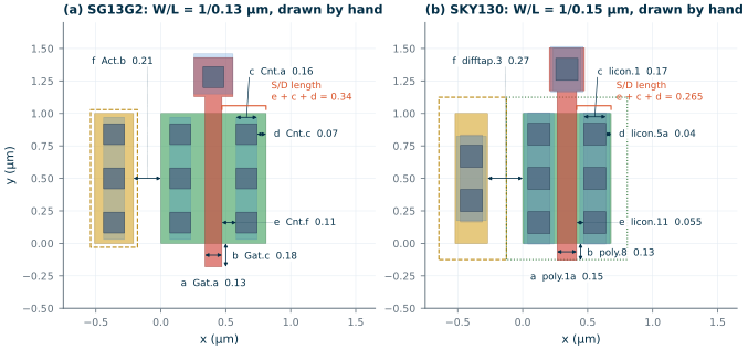
Figure 23.3 shows how few rules decide a transistor. Across the gate, the source/drain length is contact-to-gate plus contact plus enclosure: 0.11 + 0.16 + 0.07 = 0.34 µm in SG13G2, 0.055 + 0.17 + 0.04 = 0.265 µm in SKY130. Both are larger than the bare minimum the active rules allow (Act.c 0.23 µm, poly.7 0.25 µm), so the contact sets the source/drain size, not the active area. That number reappears in the transistor’s parasitics: an LVS extraction of this device reports AS = AD = 0.34 µm² in SG13G2 and 0.265 µm² in SKY130 (Section 23.7), the junction areas from which the models compute the source and drain capacitances of Chapter 4.
What this means for your design
Read every rule as a tolerance budget that someone has already paid for you, and the rules stop being arbitrary. The ones that cost area in analog layout are rarely the minimum widths, which a device at L = 0.5 µm never approaches; they are the rules between layers (contact-to-gate, enclosures, end caps), which fix the size of every source and drain, and the well rules, which fix how close a PMOS can sit to an NMOS. The 1.8 µm (SG13G2) or 1.27 µm (SKY130) of p-substrate between two n-wells on different nets is where a careless floorplan loses its area.
23.4 Density, antenna and other chip-level rules
Some rules cannot be checked on a transistor, because they depend on its surroundings. Chapter 17 explains the mechanisms and lists the limits (Tables 17.1 and 17.2); here they are in one place, with what each means for a small analog cell.
- Density. Chemical-mechanical polishing leaves sparse regions thinner than dense ones, so every layer must cover a fixed fraction of the chip and of every window. SG13G2: Activ 35–55 % of the chip and 25–65 % of every 800 × 800 µm² window, GatPoly at least 15 %, each thin metal 35–60 % globally and 25–75 % per window [16]; SKY130’s density script asks for similar windows of 700 × 700 µm² [20]. A cell alone never meets these: fill does, at chip level (Chapter 30).
- Wide metal. Above 30 µm width an SG13G2 metal needs slots (Slt.c), to relieve the mechanical stress that could lift a large plate [16].
- Antennas. During the plasma etch of each metal, a wire connected only to gates charges up and discharges through their oxide. SG13G2 limits the cumulative metal area to 200 times the gate area without a protection diode (Ant.b) and 20 000 times with one (Ant.e); SKY130’s Magic rules limit the sidewall area of each metal level to 400 times the gate area, or 2200 plus 400 per µm² of diode [16, 20]. For the minimum transistor of this chapter that is small: a gate of 0.13 µm² in SG13G2 tolerates 26 µm² of metal, about 160 µm of minimum-width Metal1; a gate of 0.15 µm² in SKY130 tolerates 60 µm² of met1 sidewall, about 80 µm of minimum-width met1 (0.36 µm thick, both sides counted).
- Latch-up distances. Every transistor must be within 20 µm (SG13G2, LU.a/b) or 15 µm (SKY130, LU.2/3) of a tie of its well or substrate. Section 23.6 shows that the rule is checked on a single transistor too.
All of these become chip-level checks: the SG13G2 antenna rules run only with run_drc.py --antenna, density with the default deck at chip level, and SKY130’s with Magic’s check_antenna.py and check_density.py. Chapter 24 treats antennas, latch-up and electromigration in depth, and Chapter 17 the tape-out checks.
23.5 Working in KLayout and Magic: grids, hierarchy, PCells and DRC
Units and grids
Both PDKs store coordinates in GDS with a database unit of 1 nm and require every vertex on a manufacturing grid of 5 nm: SG13G2 says so in its general rules (all features on a 5 nm grid; 45° angles allowed on Activ, GatPoly and the metals, only 90° on contacts and vias) [16], and the SKY130 decks check it with their off-grid rules. Magic works internally in units of 5 nm for SKY130 (the scale it reported for our runs). Set the editor grid to a multiple of 5 nm and snap to it; an odd-nanometre vertex, easy to create by scaling or by placing a cell at a computed coordinate, is a DRC error that no amount of re-drawing at the screen will reveal. The scripts of this chapter round every coordinate up to the grid (up() in hand_nmos.py).
Cells, instances and PCells
A layout is hierarchical. A cell holds shapes and instances of other cells, each with a position, rotation and mirror; an array places a cell many times on a regular grid. Hierarchy keeps files small and makes a change in one unit appear everywhere it is used, which is exactly what matched devices need (Chapter 27).
A PCell (parameterized cell) is not geometry but a program that draws geometry from parameters. In KLayout the IHP PyCells are Python classes in the library SG13_dev; a placed instance stores its parameters (w, l, ng, …) and is redrawn whenever they change [39, 14]. Magic’s SKY130 generators are Tcl procedures in sky130A.tcl, called through magic::gencell; they write an ordinary cell and keep the parameters as cell properties [40, 20]. When a layout leaves the editor as GDS, a PCell becomes plain polygons. The scripts of this chapter flatten the generated cells for the same reason: what goes to the foundry, and to DRC, is geometry.
Two editors, two models of a layout
KLayout edits GDS layers directly. Its layer properties files (sg13g2.lyp, sky130A.lyp) give each layer/datatype a name and a colour, and its technology files (.lyt) bind them to the PDK’s DRC and LVS scripts [39].
Magic edits abstract layer types. You paint ndiff (n-type diffusion), poly, or ndiffc (a contact to n-diffusion); Magic knows that poly over ndiff is an nfet and checks device rules on it as you draw. Only when it writes GDS does it generate the real layers: the cifoutput section of sky130A.tech turns ndiffc into licon cuts, li1 and the right implant, and grows every n-type active area by 0.125 µm to make nsdm (less where it butts against a p+ tie) [40, 20]. Reading GDS runs the inverse rules. This is why Magic’s DRC can check rules about devices, and why a SKY130 layout drawn in Magic needs no implant layers drawn by hand.
Running DRC from the command line
Both decks run in batch mode inside IIC-OSIC-TOOLS. These are the commands tools/layout/ch23/hand_nmos.py runs on each transistor of Section 23.6:
# IHP's KLayout deck: every rule table except density (a chip-level check)
python3 $PDK_ROOT/ihp-sg13g2/libs.tech/klayout/tech/drc/run_drc.py \
    --path=nmos_try1.gds --topcell=nmos_try1 --run_dir=drc --no_density
# -> drc/nmos_try1_nmos_try1_full.lyrdb ; 5 s for this cell
#    --table=gatpoly  runs one table; --minimum_drc only the foundry's precheck set; --antenna adds antennas
klayout nmos_try1.gds -m drc/nmos_try1_nmos_try1_full.lyrdb      # open the markers on the layout
# the KLayout deck (front and back end)
klayout -b -r $PDK_ROOT/sky130A/libs.tech/klayout/drc/sky130A_mr.drc \
    -rd input=nmos_try1.gds -rd top_cell=nmos_try1 -rd report=klayout.lyrdb \
    -rd feol=true -rd beol=true -rd offgrid=true -rd floating_met=false -rd seal=false
# Magic's full rule set: magic -dnull -noconsole -rcfile $PDK_ROOT/sky130A/libs.tech/magic/sky130A.magicrc run.tcl
#   gds read nmos_try1.gds ; load nmos_try1 ; select top cell
#   drc style drc(full) ; drc euclidean on ; drc check ; drc catchup
#   puts [drc list count total] ; puts [drc listall why]
Reading a report
KLayout writes a report database (.lyrdb, XML). Each category is a rule, with the description from the deck, and each item is one marker: a polygon or an edge pair, the two edges that are too close. The first SG13G2 attempt of Section 23.6 produces, for example,
Cnt.f   Min. Cont on Activ space to GatPoly = 0.11
        edge-pair: (0.46,0.76;0.46,0.92)/(0.41,1.018;0.41,0.662)
that is, the left edge of a drain contact at x = 0.46 µm is only 0.05 µm from the gate edge at x = 0.41 µm. In the KLayout GUI the marker browser lists the same items and zooms to each. Magic reports a message per rule, such as Diffusion contact to gate < 0.055um (licon.11), with a list of error boxes (drc listall why); interactively, drc why explains the error under the cursor, and the count it reports is of error areas, not of rule instances. Either way, read the rule name first, then find it in the rules document (section 5 of the SG13G2 layout rules [16], the SkyWater periphery rules for SKY130 [18]), and fix the shape in whatever drew it, never in the GDS (Chapter 16).
23.6 Drawing a transistor by hand
Nobody draws transistors by hand for a real design, but drawing one once is the fastest way to learn the rules. tools/layout/ch23/hand_nmos.py draws an NMOS of W = 1 µm at minimum length in both PDKs with klayout.db, rectangle by rectangle. Each coordinate is computed from a small table of rules (RULES at the top of the script, values from Table 23.4): the source/drain length from the contact rules, the number of contacts from the width, the position of the gate contact from the spacing of the first metal. It writes the GDS files, runs the DRC decks of Section 23.5 and the LVS of Section 23.7, and converts the result to a 3D model:
python3 tools/layout/ch23/hand_nmos.py       # draws, runs both PDKs' DRC, writes tools/layout/ch23/<pdk>/drc.json
python3 tools/layout/ch23/lvs_nmos.py        # LVS with and without labels -> lvs.json
python3 tools/figs/ch23_fundamentals.py      # the figures of this chapter
The first attempt
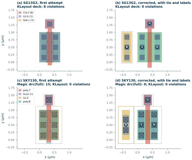
The first attempt makes three mistakes that are easy to make: the contacts are pushed against the gate (0.05 µm in SG13G2, 0.03 µm in SKY130) to save area, the gate stops 0.10 µm (SG13G2) or 0.08 µm (SKY130) beyond the active area, and there is no substrate tie, because the schematic symbol has a body terminal that “is connected to ground anyway”. Figure 23.4 and Table 23.5 show what the decks make of it.
sky130A_mr.drc passes the faulty transistor (c) with zero violations.Table 23.5. DRC of the hand-drawn transistor and of the generators' single-finger cells, IIC-OSIC-TOOLS 2026.10 (tools/layout/ch23/<pdk>/drc.json).
| Cell | SG13G2, KLayout deck | SKY130, KLayout sky130A_mr.drc |
SKY130, Magic drc(full) |
|---|---|---|---|
| First attempt | 8: Cnt.f (6), Gat.c (1), LU.b (1) | 0 | 15: licon.11, poly.7, poly.8, LU.2 |
| Corrected, with tie | 0 | 0 | 0 |
| Generator cell, 1 finger, alone | 1: LU.b | 2: met1.6 | 8: met1.6, LU.2 |
Three things stand out.
- Every mistake shows up as a rule, and the rules are the physics of Section 23.3. Cnt.f and licon.11 are the overlay budget between contact and gate; Gat.c and poly.8 the end cap; LU.b and LU.2 the latch-up distance, which a lone transistor without a tie violates by definition. SKY130 adds poly.7: pushing the contacts 0.025 µm closer to the gate shortened the source and drain to 0.24 µm, below the 0.25 µm minimum, and the rule fires along every edge.
- The SKY130 KLayout deck saw none of it.
sky130A_mr.drcchecks widths, spacings, implants and the contact and metal layers (rules such as licon.1, li.5, met1.6), but not the device rules poly.7, poly.8, licon.5 and licon.11; Magic’s full rule set does. In SKY130 run both, as Chapter 16 does for the course OTA. - The generators’ bare cells are not clean either. Without a guard ring, the IHP PyCell fails LU.b exactly like the first attempt, and Magic’s cell fails LU.2 and the minimum met1 area (met1.6) of its small gate-contact pads, which only become legal once a wire is connected to them. A generator draws a correct device, not a correct layout; ties and connections are your job.
The fix
The corrected transistor (Figure 23.4b, d) moves the contacts to exactly the minimum distance (0.11 and 0.055 µm), extends the gate by exactly the minimum end cap (0.18 and 0.13 µm), and adds a p+ tie at the minimum active spacing (0.21 µm in SG13G2, 0.27 µm in SKY130) on the source side, with its own contacts and a Metal1 terminal B. In SG13G2 the tie needs a pSD shape over its active area (enclosure 0.03 µm, pSD.c1) that stays 0.18 µm from the n+ active (pSD.d); in SKY130 a psdm shape that abuts the transistor’s nsdm. The gate contact sits on a poly head above the active area, as high as the spacing of the first metal to the source and drain stripes requires (1.20 µm above the bottom of the active area in SG13G2, 1.255 µm in SKY130). The result passes every deck with zero violations.
Common pitfall · Trusting one clean report
A clean report says only that the rules in that deck are met. The SKY130 KLayout deck passed a transistor whose contacts sat 0.03 µm from the gate and whose gate end cap was 38 % short; a bare generator cell fails latch-up and minimum-area rules that a finished layout would meet. Know what each deck checks (the SG13G2 deck lists its tables in its log; SKY130’s KLayout and Magic decks differ), run every deck the PDK offers, and treat a generator cell’s violations as a to-do list for its surroundings rather than as noise.
Against the generator
Figure 23.5 puts the hand-drawn transistor next to the generators’ cells of the same W/L, with one and two fingers, all at one scale; Table 23.6 gives the numbers.
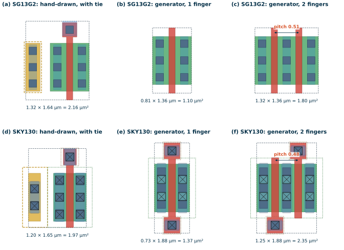
Table 23.6. Hand-drawn transistor and generator cells, W = 1 µm per finger, measured from the GDS files.
| Quantity | SG13G2 hand | SG13G2 PyCell | SKY130 hand | SKY130 Magic |
|---|---|---|---|---|
| Source/drain length, gate edge to active edge | 0.34 | 0.34 | 0.265 | 0.29 (1 finger), 0.31 (2) |
| Contacted gate pitch | 0.51 (Worked example 23.1) | 0.51 | 0.43 (Worked example 23.1) | 0.48 |
| Gate contact | one poly head | none | one poly head | one per finger, alternating top and bottom |
| Footprint without tie (µm²) | 0.81 × 1.64 = 1.33 | 0.81 × 1.36 = 1.10 | 0.68 × 1.65 = 1.12 | 0.73 × 1.88 = 1.37 |
| Footprint with tie (µm²) | 1.32 × 1.64 = 2.17 | — | 1.20 × 1.65 = 1.97 | — |
The IHP PyCell is drawn exactly at the minimum rules in the direction of the current: its active area is 0.81 × 1.00 µm, identical to the hand-drawn one, and its two-finger pitch is the minimum. It is shorter only because it leaves the gate uncontacted. Magic’s generator spends a little more: it keeps 0.06 µm between contact and active edge on all sides (the one-direction rule licon.5c applied everywhere), 0.06 to 0.08 µm between contact and gate, and draws a gate contact on every finger. Its single finger is 22 % larger than the hand-drawn one. For an analog designer that margin is cheap, and the larger spacings leave room for the rule changes a PDK goes through. The tie is what really costs area: it adds about 0.85 µm² to each hand-drawn transistor in both PDKs, nearly two thirds of the transistor’s own footprint, which is why real layouts share ties among many devices in a guard ring (Chapter 15).
Worked example 23.1 · The contacted gate pitch, by hand
Two fingers that share a contacted drain are separated by one gate length plus the drain between them. That drain must hold one contact column with the contact-to-gate spacing on each side, so the minimum gate pitch is
\[p = L + 2\,s_{cg} + c, \tag{23.4}\]with \(s_{cg}\) the contact-to-gate spacing and \(c\) the contact size. SG13G2: \(p\) = 0.13 + 2 × 0.11 + 0.16 = 0.51 µm (Gat.a, Cnt.f, Cnt.a). SKY130: \(p\) = 0.15 + 2 × 0.055 + 0.17 = 0.43 µm (poly.1a, licon.11, licon.1).
Check that no other layer is tighter. In SG13G2 the Metal1 stripes over the contacts are 0.16 µm wide, so at 0.51 µm pitch they are 0.35 µm apart, well above the 0.18 µm of M1.b. In SKY130 the li1 stripes (0.17 µm) are 0.26 µm apart against 0.17 µm (li.3), and the met1 stripes (0.23 µm, the mcon plus 0.03 µm on each side) 0.20 µm apart against 0.14 µm (met1.2). The front-end rules set the pitch in both PDKs.
The generators agree to the nanometre in SG13G2: the two-finger PyCell has its gates at 0.51 µm pitch. Magic’s two-finger cell has 0.48 µm, because it leaves 0.08 µm instead of 0.055 µm between contact and gate. The shared drain of the two fingers is (p − L) × W = 0.38 µm² in SG13G2, against 2 × 0.34 = 0.68 µm² for the drains of two separate single-finger devices: the halving of drain capacitance that Chapter 15 gets from fingers follows directly from Eq. (23.4).
In 3D
The two corrected transistors as 3D models, built from the GDS files with tools/3d/gds2glb.py and the layer stacks of the 3D gallery. Hide the metals to see the p+ tie (gold) next to the n+ active area (green), the gate end cap, and the poly head with its contact.
Drawn by hand_nmos.py from the rules of Table 23.4; 0 DRC violations; LVS matches sg13_lv_nmos W = 1 µm, L = 0.13 µm.
Drawn by hand_nmos.py; 0 violations in Magic drc(full) and in sky130A_mr.drc; LVS matches nfet_01v8 W = 1, L = 0.15.
Try it · Break the transistor one rule at a time
In
tools/layout/ch23/hand_nmos.py, changeTRY1["sky130"]todict(cont_gate=0.05), a contact only 5 nm closer to the gate than licon.11 allows, and runpython3 tools/layout/ch23/hand_nmos.py sky130. Which deck notices, and how many error tiles does Magic report? Then setW = {"sg13g2": 0.5, ...}and watch the contact columns shrink from three contacts to one, or raisecont_gateinRULES["sg13g2"]to 0.15 µm and compute the new pitch with Eq. (23.4) before you look at the GDS.
23.7 Layout as communication: names, labels, pins and notes
A layout is read by tools and by people. Both need the same things: names for the cells, names for the nets, a statement of where the terminals are, and notes on anything that is not obvious.
LVS needs labels
LVS compares the netlist extracted from the layout with the schematic’s (Chapter 16). It can find the devices without help, but it can only match the terminals of the top cell if the layout says which net is which. tools/layout/ch23/lvs_nmos.py runs LVS on the corrected transistor twice: once with its four labels, and once with the labels removed.
- With labels both tools match the layout against a one-transistor schematic. KLayout’s IHP LVS reports Netlists match and extracts
M$1 S G D B sg13_lv_nmos L=0.13u W=1u AS=0.34p AD=0.34p PS=2.68u PD=2.68u; Magic and Netgen report Circuits match uniquely withad=0.265 pd=2.53 as=0.265 ps=2.53 w=1 l=0.15[39, 40, 41]. The source/drain areas are those of Figure 23.3. - Without labels both fail. The transistor is still extracted correctly, but its nets have no names: KLayout calls them
$1to$4and stops with Netlists don’t match because the top-level ports are missing, and Netgen prints Top level cell failed pin matching, with nets named after coordinates, such asa_83_0#for the drain (83 Magic units of 5 nm = 0.415 µm, the left edge of the drain diffusion).
A net named after a coordinate changes its name whenever the geometry moves, so every report, every probe point and every post-layout netlist would be renamed by the next edit. Labels make the layout’s nets stable and readable.
Where labels and pins go
Each PDK has its own conventions (Table 23.2):
- SG13G2: a pin shape on the metal’s pin datatype (Metal1 8/2) marks the terminal area, and a text on the metal’s text datatype (Metal1 8/25) names the net; the IHP LVS deck attaches each text to the metal shape under it [14]. Pin shapes must be completely covered by drawn metal (Pin.e). The PyCells draw pin shapes themselves: the generated NMOS of Figure 23.5 carries Metal1 8/2 pins on its source and drain and a GatPoly 5/2 pin on its gate.
- SKY130: the pin datatype is 16 (met1 68/16) and the label datatype 5 (met1 68/5). Magic turns the labels into the cell’s ports when it imports the GDS, as the extracted subcircuit
nmos_hand S D B Gshows, and writes them back on export [20].
Put a label on the layer the net is meant to be connected on, at a point where the label is unambiguous: a label over two touching shapes of different nets, or on a layer that is not connected to the net at that point, is a classic source of LVS errors that look like shorts.
Notes and names for people
- Name cells after what they are (
nmos_hand,pair_abba_w9p1_l3), not after the order in which they were drawn. The cell name is the first thing a reviewer and an LVS report show. - Write notes on a text layer that never reaches a mask: SG13G2 has TEXT 63/0 for cell names and element texts, SKY130 has text 83/44. Use them for device sizes, the intended orientation of matched devices, the reason for a non-minimum spacing, and which nets are sensitive.
- Use marker and recognition layers for what tools must know. The IHP PyCell draws HeatTrans 51/0 over every gate, the layer that marks a heat source for thermal analysis [16]; resistors carry RES 24/0 or poly.res 66/13, cell outlines prBoundary. These layers are part of the description of the circuit, not decoration.
- Keep the script. A layout drawn by a script, like every layout in this part, documents itself: the rule table and the comments in
hand_nmos.pysay why each rectangle is where it is, and a regenerated layout always agrees with its documentation.
SG13G2 vs SKY130 · The same transistor, different paperwork
In SG13G2 an NMOS needs four drawn layers (Activ, GatPoly, Cont, Metal1) because n+ is the default; its tie needs a pSD shape. In SKY130 the same NMOS needs eight (diff, poly, licon, li1, mcon, met1, nsdm and npc around the gate contact), its tie two more (tap, psdm). The SKY130 transistor is still smaller, 1.12 against 1.33 µm² at the same width without tie, because its contact rules (0.055 µm to the gate, 0.04 µm enclosure) are tighter than SG13G2’s (0.11 and 0.07 µm). More layers do not mean more area, but they do mean more rules to break, and a second deck to run.
- A drawn layer is not a mask: the foundry derives masks by Boolean operations (SG13G2’s n+ implant is NOT pSD), size adjustments and OPC. Wherever you draw no Activ or diff the silicon becomes trench oxide, and the self-aligned gate sets L by the poly alone.
- The two layer sets map almost one to one, except that SKY130’s licon + li1 + mcon stack replaces SG13G2’s single Cont, SKY130 draws both implants, and SG13G2 has two thick top metals. Rule decks work on derived layers such as gate = active AND poly.
- Every rule is a budget for a physical tolerance: lithography (widths, spacings), etch (exact contact sizes), overlay (enclosures, end caps, contact-to-gate), junctions (well spacings, larger for thick oxide) and latch-up (20 µm and 15 µm to the nearest tie). The contact rules set the source/drain length: 0.34 µm in SG13G2, 0.265 µm in SKY130.
- A minimum NMOS drawn by hand passes every deck after three fixes (contact-to-gate, end cap, a substrate tie). The SKY130 KLayout deck missed all three, Magic’s drc(full) found them: run every deck.
- The contacted gate pitch L + 2 scg + c is 0.51 µm in SG13G2 (the PyCell’s pitch exactly) and 0.43 µm in SKY130 (Magic’s generator uses 0.48 µm).
- Labels and pins are part of the circuit: without them LVS fails even on a single transistor, and nets get names that change with every edit.
Further reading
- R. A. Hastings, The Art of Analog Layout [61], Chapters 2 to 4: semiconductor fabrication, layout editors and design-rule construction, and representative CMOS processes, in more depth than a web course can hold.
- J. D. Plummer, M. D. Deal and P. B. Griffin [63]: the process steps behind every mask, with lithography, implantation and etching from first principles.
- IHP, SG13G2 Layout Rules [16]: short and well illustrated; read sections 2 (the layer table), 4 (terminology and derived layers) and 5.1 to 5.16 before you draw.
- SkyWater, SKY130 PDK documentation [18]: the layer list and the periphery rules, with a figure for every rule; and the DRC section of open_pdks’
sky130A.tech[20], which is the rule set Magic actually checks. - The KLayout DRC and LVS documentation [39] and the Magic documentation [40]: how the decks compute derived layers and how to write your own checks.