Chapter 19
Sample-and-Hold Circuits
Every data converter starts by freezing its input. A switch and a capacitor do it, but the switch's resistance changes with the signal, its channel charge spills onto the capacitor when it opens, the clock decides the instant of the sample, and the capacitor leaks while it holds. This chapter measures each of these effects in both PDKs, and builds the circuits that remove most of them: bottom-plate sampling, the bootstrapped switch and the flip-around sample-and-hold.
- Describe a track-and-hold by its tracking bandwidth, acquisition time, aperture, pedestal and droop.
- Predict the distortion caused by a switch resistance that changes with the signal, and measure it with a coherently sampled FFT.
- Relate aperture jitter to the signal-to-noise ratio of a sampled sine.
- Explain how bottom-plate sampling removes the signal dependence of charge injection, and what it leaves.
- Analyse the bootstrapped switch, and size it against a transmission gate for the same on-resistance.
- Estimate droop from the off-state leakage of a switch, and design a flip-around sample-and-hold around an OTA.
Contents
19.1 What a sample-and-hold does
An analog-to-digital converter compares its input with a set of references, either all at once or one after another (Chapter 21). A successive-approximation converter takes ten or more comparisons to convert one sample, and a pipelined converter passes it through several stages; the input must not change while they do. A sample-and-hold circuit takes a sample of its input at a defined instant and keeps it constant until the converter has finished with it.
The simplest is the track-and-hold of Figure 19.1a: a switch, a hold capacitor \(C_H\) and a buffer. While the clock \(\phi\) is high the switch is on and the capacitor voltage \(V_H\) follows the input; this is the track phase. When \(\phi\) falls the switch opens and \(V_H\) keeps the value it had at that instant; this is the hold phase. (Strictly, a sample-and-hold holds its output all the time, while a track-and-hold output follows the input during track. The names are used loosely, and the circuits in this chapter are track-and-holds unless they say otherwise.)
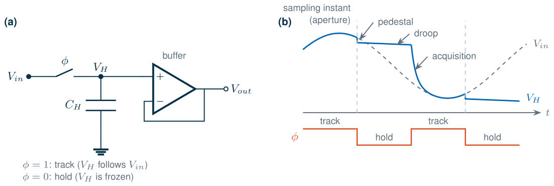
Figure 19.1b names the ways a real track-and-hold departs from an ideal sample, and the sections of this chapter take them in turn:
- Tracking (Section 19.2). In track, the switch resistance and \(C_H\) are a low-pass filter. The held voltage lags the input, and if the resistance changes with the signal, the lag distorts it.
- Acquisition time. When the switch closes, \(V_H\) must move from the old sample to the input with the time constant \(R_{on}C_H\); to settle within \(2^{-N}\) it needs \(N\ln 2\) time constants, as in Eq. (18.8).
- Aperture (Section 19.3). The sample is taken when the switch opens; uncertainty in that instant, jitter, becomes noise.
- Pedestal (Section 19.4). The switch’s channel charge and clock feedthrough step the held voltage when it opens (Eq. 18.4), by an amount that depends on the signal.
- Droop and feedthrough (Section 19.6). In hold, leakage changes the held voltage, and the input couples to it through the open switch.
Every bench in this chapter uses a 1 pF hold capacitor and an input of \(V_{DD}/2\) peak to peak around \(V_{DD}/2\) (0.3 to 0.9 V in SG13G2, 0.45 to 1.35 V in SKY130), as in Table 18.1. The open-loop benches sample at 50 MS/s, with 10 ns of track and 10 ns of hold and clock edges of 100 ps. Each switch is sized for a worst-case on-resistance of 1 kΩ over the signal range, a time constant of 1 ns, so that the capacitor settles to 10 bits in 6.9 ns, well within the track phase. The sample is read just before the end of the hold phase, as an ideal buffer would see it.
19.2 Tracking: bandwidth and distortion
In track, the switch and the hold capacitor form an RC low-pass filter with a bandwidth
\[f_{-3\,dB} = \frac{1}{2\pi R_{on}C_H}, \tag{19.1}\]159 MHz for 1 kΩ and 1 pF. For an input that changes slowly compared with this bandwidth, the held voltage lags the input by
\[v_{in} - v_H \approx R_{on}C_H\,\frac{dv_{in}}{dt}. \tag{19.2}\]If \(R_{on}\) were constant, the lag would be a small, linear phase shift and would do no harm. But the on-resistance of a MOS switch depends on the signal (Section 18.2): over the input range of our benches, the transmission gate’s resistance changes from 172 Ω to 1004 Ω in SG13G2 and from 49 Ω to 1004 Ω in SKY130. A lag proportional to a resistance that changes with the signal contains harmonics of the signal.
Suppose the resistance changes by \(\Delta R_{on}\) over the signal swing. If it peaks in the middle of the swing, as a transmission gate’s does, write \(R_{on} = R_{pk} - \Delta R_{on}\sin^2\omega t\) for an input \(V_{CM} + A\sin\omega t\). Eq. (19.2) then contains the term \(\Delta R_{on}C_HA\omega\,\sin^2\omega t\cos\omega t = \Delta R_{on}C_HA\omega\,(\cos\omega t - \cos 3\omega t)/4\), a third harmonic. If it rises steadily over the swing, the same steps give a second harmonic of the same size:
Key equation · Distortion from a signal-dependent on-resistance
\[\mathrm{HD} \approx \frac{\omega_{in}\,C_H\,\Delta R_{on}}{4}. \tag{19.3}\]HD is the amplitude of the largest harmonic relative to the signal: the third if \(R_{on}\) peaks in the middle of the swing, the second if it rises steadily. It grows by 20 dB per decade of input frequency, and it depends on the product \(C_H\,\Delta R_{on}\): a larger hold capacitor, chosen for lower kT/C noise, needs a proportionally more linear switch.
Measuring distortion
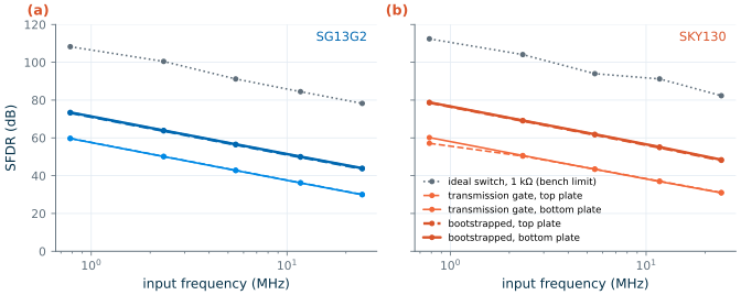
The distortion of a sampler is measured with a sine input and a fast Fourier transform (FFT) of the held samples. If the record of \(N\) samples contains exactly \(M\) cycles of the input, with \(M\) odd and \(N\) a power of two, the sine and each of its harmonics fall exactly on FFT bins, and no window is needed; this is coherent sampling. We used \(N = 64\) and \(M\) = 1, 3, 7, 15 and 31, input frequencies from 0.78 to 24.2 MHz at 50 MS/s. The spurious-free dynamic range (SFDR) is the ratio of the signal to the largest other component of the spectrum, and the total harmonic distortion (THD) is the ratio of all the harmonics together to the signal. To check the bench itself, an ideal switch with a constant 1 kΩ, the same RC as the real switches, samples the same input; its SFDR, 78 dB or more at every frequency, is the limit of the bench’s accuracy, and far above every real switch.
Figure 19.2 shows the spectra of the transmission-gate track-and-hold. At 2.3 MHz the largest harmonic is 50 dB below the signal in both PDKs. At 24.2 MHz, near the Nyquist frequency \(f_s/2\), the second harmonic is only 30 dB below it in SG13G2 and 31 dB in SKY130, and the third 35 and 37 dB: a 5-bit sampler. Both harmonics appear because the gate’s resistance peaks above the centre of the swing rather than at it. Harmonics above \(f_s/2\) fold back into the band, as every component of a sampled signal does: the third harmonic of 24.2 MHz, at 72.7 MHz, appears at 72.7 − 50 = 22.7 MHz, next to the signal, and the second at 50 − 48.4 = 1.6 MHz.
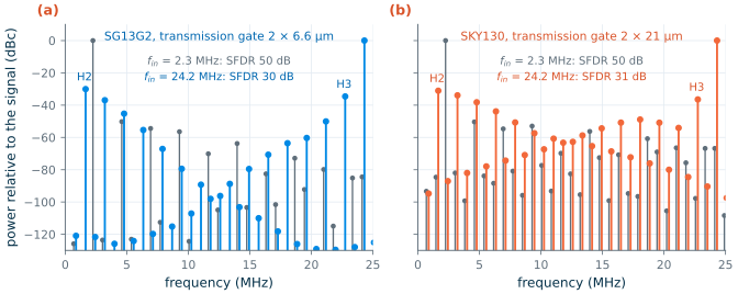
Eq. (19.3) predicts these numbers well. With \(\Delta R_{on}\) = 832 Ω it gives an SFDR of 59.8 dB at 0.78 MHz in SG13G2 and 30.0 dB at 24.2 MHz; the simulations give 59.8 and 30.1 dB. In SKY130 (\(\Delta R_{on}\) = 955 Ω) it gives 58.6 and 28.8 dB, against 57.1 and 31.1 dB simulated: the sharp peak of the SKY130 gate covers less of the swing than a smooth curve with the same \(\Delta R_{on}\) would. The prediction works because the tracking error is much larger than the other errors of the sampler; Section 19.4 measures the next one.
SG13G2 vs SKY130 · The same resistance costs SKY130 three times the width
For a worst-case on-resistance of 1 kΩ over its swing, the SKY130 transmission gate needs two 21 µm devices, the SG13G2 gate two 6.6 µm devices, because of the weaker SKY130 PMOS and narrower overlap of Figure 18.2. The wide devices conduct very well near the ends of the swing (49 Ω at 0.45 V), so the SKY130 gate’s resistance changes by more (955 against 832 Ω), but over a narrower peak, and the two gates distort about equally (Figure 19.8). The real cost of the width is the channel charge, three times larger, which Section 19.4 measures.
19.3 Aperture jitter
The sample is taken at the instant the switch opens. Any uncertainty in that instant, from jitter of the clock edge or noise on the edge that drives the switch, becomes an error in the sample proportional to the slope of the input. For a sine of amplitude \(A\) and angular frequency \(\omega\), a timing error of rms value \(\sigma_t\) gives a voltage error of rms value \(A\omega\sigma_t/\sqrt 2\), and the signal-to-noise ratio is
\[\mathrm{SNR}_{jitter} = -20\log_{10}\left(2\pi f_{in}\,\sigma_t\right). \tag{19.4}\]It depends on neither the amplitude nor the sampling rate, only on the product of the input frequency and the jitter [94]. Figure 19.3 plots it for three values of jitter, with the result of a behavioural Monte Carlo simulation that samples a sine at randomly displaced instants (dots, 8 records of 4096 samples each); the two agree within 0.3 dB. The dashed lines are the kT/C noise of a 1 pF capacitor for the signal swings of our benches, 70.4 dB in SG13G2 and 73.9 dB in SKY130: jitter matters once its line falls below them.
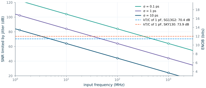
A 10-bit converter needs an SNR of about 62 dB (Chapter 21). At an input of 25 MHz, Eq. (19.4) allows 5 ps of jitter; at 250 MHz, 0.5 ps. The jitter of the clock source, an oscillator or phase-locked loop, is the subject of Chapter 22. The circuit that drives the switch adds its own: a noise voltage \(\sigma_v\) on an edge of slope \(dV/dt\) moves the edge by \(\sigma_v/(dV/dt)\), so the sampling clock should have fast edges and should not share a supply with noisy logic. The edge also defines which voltage starts the hold: an NMOS switch opens when its gate falls to \(V_{in} + V_{TH}\), so with a finite edge rate the sampling instant moves with the signal. That error is deterministic, a signal-dependent aperture delay, and both circuits of the next two sections largely remove it: bottom-plate sampling lets a switch at a fixed voltage define the instant, and a bootstrapped gate always falls through the same voltage before its switch opens.
19.4 Bottom-plate sampling
When a switch opens, its channel charge divides between the hold capacitor and the input (Section 18.3). The channel charge \(WLC_{ox}(V_{DD} - V_{in} - V_{TH})\) depends on the signal, so the pedestal does too, and a pedestal that changes nonlinearly with the signal is distortion.
Bottom-plate sampling (Figure 19.4) makes the sampled charge independent of the input switch [93]. The hold capacitor sits between the input switch (plate A) and the amplifier’s inverting input (plate B). In phase \(\phi_1\) the amplifier is a follower, so B is at \(V_{CM}\) and \(C_H\) charges to \(V_{in} - V_{CM}\). The switch at B, driven by the early phase \(\phi_{1e}\), opens first. From that instant B is floating, and the charge on it, \(C_H(V_{CM} - V_{in})\) plus the charge injected by the B switch, can no longer change. The B switch always opens at the same voltage, \(V_{CM}\), so its injection is a constant offset. When the input switch opens a moment later, its channel charge can only flow to the input source and to plate A, whose voltage the floating plate B no longer fixes; it changes nothing on B. In phase \(\phi_2\) plate A is connected to the output, the amplifier restores B to \(V_{CM}\), and the output becomes the sampled input: this is the flip-around sample-and-hold of Section 19.7.
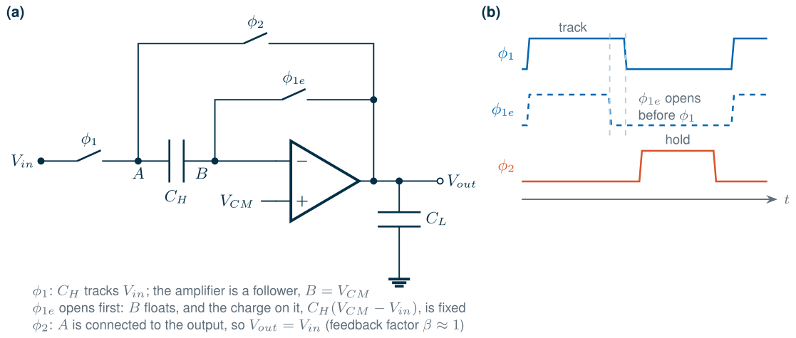
To measure the effect of the switches alone, we built the circuit of Figure 19.4 with an ideal amplifier (a transconductance amplifier with a gain of 104 and a unity-gain frequency of 1.6 GHz) and compared it with the top-plate track-and-hold of Figure 19.1, both with the 1 kΩ switches of Section 19.2. Figure 19.5 shows the sampling error for DC inputs across the swing. With top-plate sampling, the transmission gate’s error changes by 2.1 mV over the swing in SG13G2 and 12.9 mV in SKY130, where the 21 µm devices carry three times the channel charge. With bottom-plate sampling, the change falls to 0.06 and 0.10 mV, and what remains is a straight line, the ideal amplifier’s gain error of 10−4. After a straight line is removed, the nonlinear part of the error falls from 0.091 to 0.0012 mV in SG13G2 and from 1.4 to 0.0047 mV in SKY130, 75 and 300 times less. The price is a constant offset, the B switch’s own pedestal, of +0.97 mV and +7.4 mV, which a differential circuit cancels.
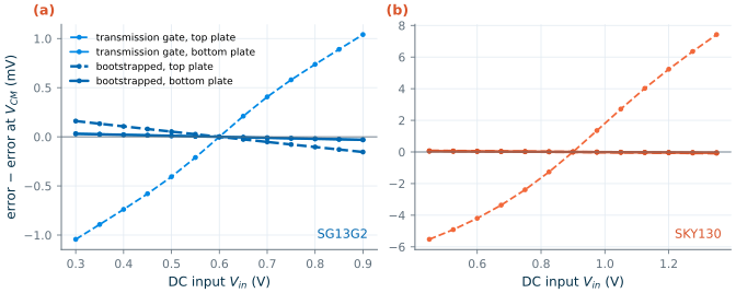
Bottom-plate sampling does nothing for the tracking error of Section 19.2, which is set while the switch is still on. In our benches the tracking error dominates at every input frequency, and bottom-plate sampling changes the SFDR of Figure 19.8 by less than 0.3 dB, with one exception: the SKY130 transmission gate at the lowest frequency, 0.78 MHz, where its large charge injection still matters and bottom-plate sampling gains 3 dB. The two errors need two remedies: bottom-plate sampling for the charge, and a switch with a constant resistance for the tracking.
19.5 The bootstrapped switch
The on-resistance and the channel charge of a MOS switch both depend on its overdrive, \(V_{GS} - V_{TH}\). A gate held at \(V_{DD}\) gives an overdrive that falls as the input rises. A bootstrapped switch drives the gate to \(V_{in} + V_{DD}\) instead, so that \(V_{GS}\) stays at about \(V_{DD}\) for every input [95, 97]. It does this with a capacitor \(C_b\) that is charged to \(V_{DD}\) in hold and then placed, like a battery, between the input and the gate in track (Figure 19.6). Charge sharing with the gate’s capacitance \(C_p\) (the main switch’s gate and the parasitics of the gate node) reduces the boost slightly:
\[V_G = V_{in} + V_{DD}\,\frac{C_b}{C_b + C_p}. \tag{19.5}\]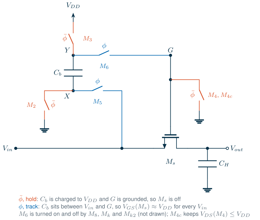
Our version, after Abo and Gray [95], adds nine helper transistors of 1 µm, minimum length, and \(C_b\) = 0.2 pF to the main switch \(M_s\):
- In hold, \(M_2\) grounds the bottom plate X and \(M_3\) connects the top plate Y to \(V_{DD}\), so \(C_b\) charges to \(V_{DD}\). \(M_4\) grounds the gate G through the cascode \(M_{4c}\), whose gate is at \(V_{DD}\): in track G rises to almost \(2V_{DD}\), and the cascode shares that voltage with \(M_4\) so that neither sees much more than \(V_{DD}\).
- In track, \(M_5\) connects X to the input and the PMOS \(M_6\) connects Y to G. \(M_6\)’s gate is pulled to X by \(M_k\) (gate at \(\phi\)) and \(M_{k2}\) (gate at G, so that it conducts for any input), and pulled up to \(V_{DD}\) by \(M_8\) in hold. \(M_3\)’s gate is G, which turns it off once G rises above \(V_{DD}\); its n-well is tied to Y, the highest voltage in the circuit.
Figure 19.7a shows the result. Over the whole input range, 0 to \(V_{DD}\), the main switch’s \(V_{GS}\) stays between 1.12 and 1.13 V in SG13G2 (93 % of \(V_{DD}\)) and between 1.71 and 1.72 V in SKY130 (95 %), while the NMOS of a transmission gate sees \(V_{DD} - V_{in}\). Over the signal swing, the on-resistance (b) changes from 842 to 998 Ω in SG13G2 and from 863 to 950 Ω in SKY130, against 172 to 1004 Ω and 49 to 1004 Ω for the transmission gates. What remains is the body effect: the main switch’s source follows the input, but its body stays at ground, so its threshold rises with the input. For the same worst-case resistance the main NMOS is 1.0 µm wide in SG13G2 and 0.92 µm in SKY130, against 2 × 6.6 µm and 2 × 21 µm for the transmission gates; less gate area means less channel charge, which is why the bootstrapped switch’s DC error in Figure 19.5 is small even with top-plate sampling.
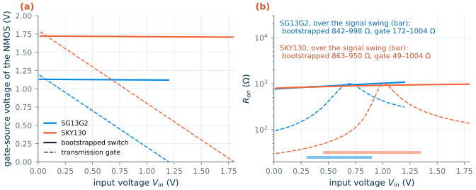
Figure 19.8 shows what this buys. Every curve falls by 20 dB per decade, as Eq. (19.3) says. The bootstrapped switch is 13.5 dB better than the transmission gate in SG13G2 and 17 to 21 dB better in SKY130, close to the ratios of their \(\Delta R_{on}\) (832/156, 14.5 dB, and 955/87, 20.8 dB). At 24.2 MHz it reaches 43.7 dB in SG13G2 and 48.1 dB in SKY130, where Eq. (19.3) predicts 44.6 and 49.6 dB. Its distortion is almost all second harmonic, because its resistance rises steadily with the input; the third harmonic is 65 dB (SG13G2) and 58 dB (SKY130) below the signal, and a differential sampler, which cancels the even harmonics, would reach about that.
What this means for your design
- The sampling switch sets the linearity of the whole converter. Nothing after the sample can remove its distortion. Eq. (19.3) says that the product \(C_H\,\Delta R_{on}\) must fall in proportion to the target distortion and to the input frequency, so a high-resolution, high-frequency sampler needs both a large \(C_H\) (for kT/C noise) and a switch whose resistance hardly changes: a bootstrapped switch.
- Remove charge errors with timing, resistance errors with bootstrapping. Bottom-plate sampling makes the sampled charge independent of the input switch, but only a constant \(V_{GS}\) makes the tracking error linear.
- What limits the bootstrapped switch is the body effect. In a process with isolated p-wells (a deep n-well), the main switch’s body can be switched to its source as well, which removes the body effect.
19.6 Hold mode: droop and feedthrough
In hold, the switch is off but not perfect. The current that still flows through it, subthreshold current through the channel and the reverse current of its junctions, changes the held voltage at a rate
\[\frac{dV_H}{dt} = \frac{I_{leak}}{C_H}. \tag{19.6}\]We simulated the leakage of each switch with the hold node at \(V_{CM}\) and the input at 0 or \(V_{DD}\), whichever gives more current, at 27 °C and 125 °C (Table 19.1). Almost all of it is subthreshold current: through the NMOS when the input is low, through the PMOS when it is high.
Table 19.1. Off-state leakage and droop of the 1 kΩ switches of this chapter on CH = 1 pF (hold node at VCM, input at 0 or VDD, whichever leaks more), and the longest hold for an error of half an LSB at 10 bits (full scale VDD/2).
| SG13G2 gate (2 × 6.6 µm) | SG13G2 bootstrapped (1.0 µm) | SKY130 gate (2 × 21 µm) | SKY130 bootstrapped (0.92 µm) | |
|---|---|---|---|---|
| Leakage, 27 °C | 200 pA | 16 pA | 149 pA | 1.0 pA |
| Droop, 27 °C | 0.20 mV/µs | 0.016 mV/µs | 0.15 mV/µs | 0.001 mV/µs |
| Longest 10-bit hold, 27 °C | 1.5 µs | 18 µs | 3.0 µs | 460 µs |
| Leakage, 125 °C | 11 nA | 1.0 nA | 69 nA | 27 pA |
| Droop, 125 °C | 11 mV/µs | 1.0 mV/µs | 69 mV/µs | 0.027 mV/µs |
| Longest 10-bit hold, 125 °C | 26 ns | 0.29 µs | 6.4 ns | 16 µs |
At room temperature every switch holds a 10-bit sample for at least a microsecond, far longer than the 10 ns hold of a 50 MS/s sampler. Leakage, however, grows steeply with temperature, by a factor of 56 for the SG13G2 transmission gate and 460 for the SKY130 one between 27 °C and 125 °C, and at 125 °C the SKY130 transmission gate cannot hold a 10-bit sample for longer than 6.4 ns. The narrow bootstrapped switches leak far less, because for the same on-resistance they are 13 to 46 times narrower. Droop matters most in slow converters, whose sample must survive many comparisons: a 1 MS/s successive-approximation converter holds each sample for about a microsecond.
SG13G2 vs SKY130 · Which switch leaks
At 27 °C the SG13G2 NMOS leaks much more per micrometre of width than the SKY130 NMOS: the 1.0 µm bootstrapped switch leaks 16 pA in SG13G2 and 1.0 pA in SKY130, the same difference that made the SG13G2 integrator of Section 18.5 need a reset phase. At 125 °C the order of the transmission gates changes: the SKY130 PMOS, 21 µm wide, leaks 69 nA when the input is at VDD, six times more than the whole SG13G2 gate. Check the leakage of every switch at the hottest corner the chip must work at, not at 27 °C.
Hold-mode feedthrough is the coupling from the input to the held node through the open switch. With the gate held firmly off, the compact models give almost no coupling through the channel: below −140 dB in both PDKs. In a real circuit the coupling is set by the layout, by the capacitance between the input wiring and the hold node, and 1 fF of it on 1 pF is −60 dB.
Common pitfall · Trusting the simulated feedthrough
A schematic simulation shows almost perfect isolation in hold, because the transistor models have almost no capacitance between the drain and source of an off device. Extract the layout (Chapter 15) and simulate again: the wires that bring the input to the switch and take the held voltage away run side by side, and their coupling capacitance is the feedthrough. Keep them apart, shield the hold node, and in a differential circuit add cross-coupled dummy capacitors that cancel it.
19.7 A closed-loop sample-and-hold
The open-loop track-and-hold needs a buffer that can drive the next stage without loading \(C_H\), and a source follower or an op-amp follower adds its own offset and distortion. The flip-around sample-and-hold of Figure 19.4 puts the amplifier in a feedback loop instead. In hold, \(C_H\) is connected between the amplifier’s output and its inverting input, so the feedback factor is
\[\beta = \frac{C_H}{C_H + C_{in}}, \qquad V_{out} = \frac{V_{in}}{1 + 1/(\beta A_0)}, \qquad \tau = \frac{1}{2\pi\beta f_u}, \tag{19.7}\]where \(C_{in}\) is the input capacitance of the amplifier and the parasitic of plate B. With \(C_{in} \ll C_H\), \(\beta\) is close to 1, larger than in any other switched-capacitor stage: the flip-around circuit is the fastest closed-loop sample-and-hold for a given amplifier [98]. The other common circuit, the charge-redistribution sample-and-hold, samples on one capacitor and transfers the charge to a second one of the same size, with \(\beta \approx 1/2\) and twice the kT/C noise. In the flip-around circuit the amplifier’s offset is sampled in \(\phi_1\) and subtracted in \(\phi_2\), as in the gain stage of Section 18.6.
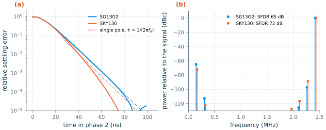
We built it around the course OTA of Chapter 12 with the bootstrapped input switch, \(C_H\) = 1 pF, a 1 pF load and a clock of 5 MS/s, which leaves 99 ns for the hold phase. Figure 19.9a shows the settling for a step of 100 mV either side of \(V_{CM}\). After the first 20 ns, in which the switches close and the output starts to move, the error falls along a straight line: τ = 7.3 ns in SG13G2, against 7.4 ns from Eq. (19.7) with β = 1 and the fu of Chapter 12; in SKY130 the tail is faster, 5.4 ns. The output settles to 0.1 % in 61 ns (SG13G2) and 54 ns (SKY130). The gain errors are −0.057 % and −0.076 %, against 1/(βA0) = 0.078 % and 0.016 %. With an ideal amplifier in place of the OTA, the same circuit and switches give −0.010 %, the ideal amplifier’s own 1/A, so the switches contribute nothing measurable and the rest is the OTA; in SKY130 its gain over the output excursion is lower than its small-signal A0, about 62 dB instead of 75.7 dB. The spectrum (b) for an input at 2.42 MHz has an SFDR of 64.9 dB in SG13G2 and 72.2 dB in SKY130, set by the second harmonic. Eq. (19.3) with the bootstrapped switches’ \(\Delta R_{on}\) predicts 64.6 and 69.7 dB at this frequency: the input switch, not the OTA, limits the linearity.
Worked example 19.1 · A 10-bit, 5 MS/s sample-and-hold with the course OTA
Specification. Ten bits (an SNDR of at least 62 dB) for inputs up to the Nyquist frequency of 2.5 MHz, a swing of \(V_{DD}/2\) peak to peak, \(C_H\) = 1 pF.
Hand estimates. Noise: the kT/C noise of 1 pF limits the SNR to 70.4 dB in SG13G2 and 73.9 dB in SKY130 (Figure 19.3), 8 and 12 dB above the target. Jitter: at 2.5 MHz, Eq. (19.4) allows \(\sigma_t = 10^{-62/20}/(2\pi\cdot 2.5\ \text{MHz})\) = 50 ps, far more than an on-chip clock has. Switch: for distortion below −62 dB at 2.5 MHz, Eq. (19.3) allows \(C_H\Delta R_{on} \le 4\cdot 10^{-62/20}/(2\pi\cdot 2.5\ \text{MHz})\) = 0.20 ns, so \(\Delta R_{on} \le\) 200 Ω: the bootstrapped switches (156 and 87 Ω) pass, the transmission gates (832 and 955 Ω) do not. Settling: with β ≈ 1, τ = 7.4 ns, and 10 bits need \(10\ln 2\,\tau\) = 51 ns, half the 99 ns hold phase. Gain: \(1/(\beta A_0)\) = 0.078 % and 0.016 %, below \(2^{-10} \approx\) 0.1 %.
Simulation. Settling to 0.1 % takes 61 and 54 ns, the gain errors are −0.057 % and −0.076 %, and the SNDR at 2.42 MHz is 64.9 dB (10.5 bits) in SG13G2 and 72.1 dB (11.7 bits) in SKY130. A transient simulation has no noise: adding the kT/C noise of 1 pF gives 63.8 and 69.9 dB, or 10.3 and 11.3 bits, before the OTA’s own noise.
What limits it. In SG13G2, the bootstrapped switch’s second harmonic and the kT/C noise together leave only 1.8 dB of margin. Doubling the switch width would halve \(\Delta R_{on}\), about 6 dB by Eq. (19.3), and a differential version would cancel the second harmonic altogether. Settling is not the limit yet: a 100 mV step needs 61 ns of the 99 ns available, and a full-scale step adds about 20 ns of slewing (0.3 V at 15 V/µs).
Try it · The sample-and-hold script
Every number in this chapter comes from
tools/figs/ch20_sample_hold.py, which runs its parts separately:python3 tools/figs/ch20_sample_hold.py ron dcerr. The SFDR sweep takes about half an hour and caches its samples; deletetools/_work/ch20_sweep.jsonto run it again. Try three changes. (1) Double the transmission-gate width (W_TG): \(\Delta R_{on}\) halves, so Eq. (19.3) predicts 6 dB more SFDR. Is that what the sweep gives, and does the DC error of Figure 19.5 double? (2) Make the bottom-plate switch open at the same time as the input switch (T_EARLY = 0) and rundcerr. (3) Halve the boost capacitor (bsw(..., cb=0.1e-12)) and see how \(V_{GS}\) in Figure 19.7 changes, against Eq. (19.5).
- A track-and-hold is a switch, a capacitor and a buffer; its errors are the tracking lag, the acquisition time, the aperture, the pedestal, droop and feedthrough.
- A switch resistance that changes by \(\Delta R_{on}\) over the swing causes a harmonic of about \(\omega_{in}C_H\Delta R_{on}/4\) (Eq. 19.3), which predicts the simulated SFDR within 2.5 dB: a 1 kΩ transmission gate on 1 pF reaches only 30–31 dB at 24 MHz in either PDK.
- Jitter limits the SNR to \(-20\log_{10}(2\pi f_{in}\sigma_t)\), whatever the amplitude and the sampling rate; 10 bits at 25 MHz need 5 ps.
- Bottom-plate sampling makes the sampled charge independent of the input switch: the nonlinear part of the DC error fell 75 times in SG13G2 and 300 times in SKY130. It does nothing for the tracking error.
- The bootstrapped switch keeps \(V_{GS}\) at 93–95 % of \(V_{DD}\) for every input; for the same worst-case resistance it is 13 to 46 times narrower than a transmission gate, 13 to 21 dB more linear, and leaks less.
- Off-state leakage sets the droop \(I_{leak}/C_H\) and grows by up to 460 times from 27 °C to 125 °C; at 125 °C the 2 × 21 µm SKY130 gate holds a 10-bit sample for only 6.4 ns.
- The flip-around sample-and-hold has β ≈ 1: with the course OTA it settles to 0.1 % in 54–61 ns, and at 5 MS/s it reaches 10.5 bits (SG13G2) and 11.7 bits (SKY130), limited by the input switch rather than by the OTA.
Further reading
- B. Razavi’s two columns on the bootstrapped switch [99, 100]: how it works, and a step-by-step design with its reliability constraints.
- A. M. Abo and P. R. Gray [95]: the bootstrapped switch in a low-voltage pipelined ADC, with the care for oxide stress that every later version follows; M. Dessouky and A. Kaiser [97] apply the same idea to every switch of a 1 V converter.
- S. H. Lewis and P. R. Gray [93]: a pipelined ADC whose fully differential sample-and-hold uses bottom-plate sampling with an early clock phase.
- M. Shinagawa, Y. Akazawa and T. Wakimoto [94] on jitter in sampling systems, and R. H. Walden’s survey [96], which shows how aperture jitter limits the resolution of real converters.
- T. Chan Carusone, D. A. Johns and K. W. Martin, Analog Integrated Circuit Design [52], the chapter on sample-and-holds and comparators.