Chapter 3
Two Open PDKs: SG13G2 and SKY130
IHP's SG13G2 and SkyWater's SKY130 are both 130 nm processes, but they differ in supply voltage, device models and metal stack. Knowing those differences tells you why the same circuit sizes out differently in each.
- Sketch the cross-section of a 130 nm CMOS process and name its layers.
- List the analog devices of SG13G2 and SKY130 and their voltage ratings.
- Explain how ngspice finds the models, what the corner sections mean, and why SG13G2 needs OSDI.
- Compare the two PDKs’ core transistors using simulated data.
Contents
See the devices in 3D
This chapter describes the devices of both PDKs in words, numbers and cross-sections. The gallery PDK Devices in 3D shows the same transistors, resistors and capacitors as interactive 3D models built from the PDKs’ own layouts and layer stacks. Keep it open in a second tab while you read.
3.1 Inside a 130 nm process
“130 nm” names a technology generation: the shortest gate a process of that generation can draw is about 0.13 µm. Both of our processes belong to it, and both are built the same way, in two parts.
The front end of line (FEOL) is everything made in and on the silicon wafer: the transistors. Shallow trenches filled with oxide (shallow trench isolation, STI) separate the active areas. Implanted wells set the doping under each transistor: p-wells for NMOS and n-wells for PMOS. A few nanometres of gate oxide are grown, a polysilicon gate is patterned on top, and heavy implants on both sides of the gate form the source and drain. Finally, a thin metal silicide is formed on the exposed silicon and poly to lower their resistance, except where a salicide block layer keeps it off, which is how high-value poly resistors are made.
The back end of line (BEOL) is the wiring: layers of metal separated by oxide and connected by vertical plugs called contacts (to silicon and poly) and vias (between metals). The BEOL also holds the metal-insulator-metal (MIM) capacitors, a thin dielectric between a metal layer and an extra top plate.
Figure 3.1 compares the BEOL of the two processes to scale, using the layer thicknesses published in each PDK [15, 18]. The transistors live in the bottom few hundred nanometres, below the first metal.
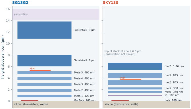
Three differences stand out.
- SG13G2’s two thick top metals, TopMetal1 (2 µm) and TopMetal2 (3 µm), have sheet resistances of only 18 and 11 mΩ/□, against 88–110 mΩ/□ for the thin Metal1–Metal5 [15]. They are there for power distribution and for the low-loss inductors and transmission lines of the process’s radio-frequency circuits.
- SKY130 has a local interconnect, li1, a thin (100 nm) conducting layer between poly and met1. Contacts to silicon and poly (licon) land on li1, and a second contact (mcon) connects li1 to met1. It makes dense cells easy to wire, but it is resistive, so analog layouts use it only for short connections.
- The SKY130 stack is shorter, about 6.6 µm from silicon to the top of met5 against 13.8 µm to the top of TopMetal2 in SG13G2. Wire-to-substrate capacitances differ accordingly; Chapter 15 quantifies them.
3.2 IHP SG13G2
SG13G2 is IHP’s 130 nm SiGe:C BiCMOS process: a CMOS process with high-speed silicon-germanium heterojunction bipolar transistors (HBTs) added. It offers two gate oxides, a thin one for 1.2 V logic and a thick one for 3.3 V, NMOS, PMOS and isolated NMOS devices for each, poly resistors and MIM capacitors, five thin aluminium metal layers and two thick ones [15]. Table 3.1 lists the devices an analog designer uses most, with their names in the PDK’s Xschem library.
Table 3.1. Main analog devices of SG13G2 [15, 16].
| Device | PDK name | Rating and key data |
|---|---|---|
| Core NMOS / PMOS | sg13_lv_nmos, sg13_lv_pmos |
1.2 V; L ≥ 0.13 µm; oxide 2.65 / 2.45 nm |
| Thick-oxide NMOS / PMOS | sg13_hv_nmos, sg13_hv_pmos |
3.3 V; L ≥ 0.45 / 0.40 µm; oxide 7.5 / 7.3 nm |
| SiGe HBT | npn13G2 (also npn13G2l, npn13G2v) |
fT = 350 GHz, fmax = 450 GHz, β ≈ 650, BVCEO = 1.6 V |
| Lateral PNP | pnpMPA |
for bandgap references |
| Salicided poly resistor | rsil |
7.0 Ω/□ |
| Unsalicided p+ poly resistor | rppd |
260 Ω/□ |
| High-resistance poly resistor | rhigh |
1360 Ω/□ |
| MIM capacitor | cap_cmim |
1.5 fF/µm², between Metal5 and TopMetal1 |
| Varactor, diodes, ESD | sg13_svaricap, … |
The HBT is what makes SG13G2 special: with a transit frequency of 350 GHz it is one of the fastest devices in any open PDK, and it is the reason the process exists. For the CMOS analog circuits of this course, the important devices are the 1.2 V core transistors, and they have a character of their own. Their oxide is thin and their channels heavily doped near the source and drain (halo implants), which makes their threshold voltage rise sharply at short lengths: in the process specification the NMOS threshold is 0.50 V at L = 0.13 µm but only 0.20 V at L = 10 µm [15]. As Chapter 6 showed, the same physics limits their intrinsic gain.
The models of the core and thick-oxide transistors use PSP 103.6, a surface-potential-based compact model [73]. PSP is not built into ngspice; it is written in Verilog-A, compiled with OpenVAF into a shared library (psp103.osdi) and loaded at start-up through the OSDI interface [42, 37] (Section 3.5). The model files state their valid range: L from 0.13 to 10 µm, W from 0.15 to 10 µm, and a maximum drain-source voltage of 1.5 V for the core devices.
3.3 SkyWater SKY130
SKY130 is SkyWater Technology’s 130 nm CMOS process, released as an open PDK with Google in 2020 [18]. It is a mixed-signal process with a wide range of voltages: 1.8 V core devices, 5 V/10.5 V devices for I/O and power, and 20 V devices, plus SONOS memory cells. Table 3.2 lists the main analog devices.
Table 3.2. Main analog devices of SKY130 [18, 19]. All names carry the prefix sky130_fd_pr__.
| Device | PDK name | Rating and key data |
|---|---|---|
| Core NMOS / PMOS | nfet_01v8, pfet_01v8 |
1.8 V; L ≥ 0.15 µm; oxide 4.15 nm (model toxe) |
| Low- and high-VTH variants | nfet_01v8_lvt, pfet_01v8_lvt, pfet_01v8_hvt |
1.8 V |
| 5 V / 10.5 V NMOS / PMOS | nfet_g5v0d10v5, pfet_g5v0d10v5 |
5 V gate, up to 10.5 V drain |
| Native NMOS | nfet_03v3_nvt, nfet_05v0_nvt |
threshold near zero |
| Bipolar | npn_05v5, pnp_05v5 |
parasitic devices, β ≈ 38 (NPN) and 13 (PNP) |
| Generic poly resistor | res_generic_po |
48.2 Ω/□ |
| Precision p+ poly resistor | res_high_po_0p35 … _5p73 |
about 300 Ω/□, fixed widths 0.35 to 5.73 µm |
| Precision p− poly resistor | res_xhigh_po_0p35 … _5p73 |
about 2000 Ω/□, same widths |
| MIM capacitor | cap_mim_m3_1, cap_mim_m3_2 |
2 fF/µm², above met3 or met4 |
SKY130 has no fast bipolar transistor; its NPN and PNP are by-products of the wells, good enough for bandgap references (Chapter 14). Its strength for analog work is the 1.8 V core transistor: the thicker oxide and longer minimum length give it a much higher intrinsic gain than the SG13G2 core device, and the 1.8 V supply leaves more room for signals.
The SKY130 transistor models are BSIM4 (level 54, version 4.5), which ngspice has built in, so no extra library is needed. They are binned: the nfet_01v8 model of the original library is really 180 models, each fitted for a small range of W and L, and the simulator picks the bin that contains the device you draw (Section 3.5). The precision resistors come only in fixed widths, because they were characterized only at those widths.
3.4 Side by side
How different are the two core transistors? Figure 3.2 shows the simulated drain current per micrometre of width of minimum-length NMOS and PMOS devices, 10 µm wide, with gate and drain both at the full supply. We measured the threshold voltage the way IHP’s process control does it [15]: at \(\vert V_{DS}\vert\) = 50 mV, extrapolate the \(I_D(V_{GS})\) curve linearly from its point of steepest slope down to zero current, at a gate voltage \(V_0\), and correct for the drain voltage,
\[V_{TH} = V_0 - \frac{V_{DS}}{2}. \tag{3.1}\]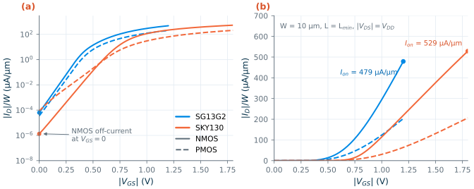
Table 3.3 collects the main numbers. Where the process specification gives a value, our simulation reproduces it closely: for the SG13G2 NMOS, a threshold of 0.500 V (specified 0.50 V), an on-current of 479 µA/µm (480 µA/µm) and a subthreshold slope of 83 mV/decade (82 mV/decade) [15].
Table 3.3. The two PDKs side by side. Device values are our simulations (tt, 27 °C, W = 10 µm, threshold by Eq. 3.1); process values are from the PDK documents [15, 16, 18].
| Quantity | SG13G2 | SKY130 |
|---|---|---|
| Core supply \(V_{DD}\) | 1.2 V | 1.8 V |
| Minimum drawn L of core devices | 0.13 µm | 0.15 µm |
| Gate oxide of core devices | 2.65 nm (NMOS), 2.45 nm (PMOS) | 4.15 nm (model) |
| NMOS \(V_{TH}\) at Lmin / at L = 10 µm | 0.500 V / 0.201 V | 0.724 V / 0.547 V |
| PMOS \(\vert V_{TH}\vert\) at Lmin / at L = 10 µm | 0.461 V / 0.354 V | 0.805 V / 1.05 V |
| NMOS / PMOS on-current at \(V_{DD}\) | 479 / 203 µA/µm | 529 / 206 µA/µm |
| NMOS / PMOS off-current at \(V_{DD}\) | 63 / 35 pA/µm | 1.3 / 85 pA/µm |
| NMOS subthreshold slope | 83 mV/decade | 91 mV/decade |
| Higher-voltage devices | 3.3 V thick oxide | 5 V / 10.5 V, 20 V |
| Bipolar | SiGe HBT, fT 350 GHz | parasitic NPN and PNP |
| Metal layers | Metal1–5 + TopMetal1 (2 µm) + TopMetal2 (3 µm) | li1 + met1–5 (met5 1.26 µm) |
| Poly resistors | 7, 260, 1360 Ω/□ | 48, 300, 2000 Ω/□ |
| MIM capacitor | 1.5 fF/µm² | 2.0 fF/µm² |
The table holds a surprise. Although SG13G2 runs from a supply one third lower, its NMOS delivers almost the same on-current per micrometre as SKY130’s (479 against 529 µA/µm, 10 % less), because its thinner oxide gives each volt of gate drive more charge. What the lower supply costs is headroom: an SG13G2 NMOS turns on at 0.5 V out of 1.2 V, a SKY130 NMOS at 0.72 V out of 1.8 V. Notice also how the thresholds depend on length. Both NMOS thresholds fall from Lmin to L = 10 µm, by 0.30 V in SG13G2 but 0.19 V in SKY130; the SG13G2 PMOS threshold falls too, while the SKY130 PMOS threshold rises, the classic short-channel roll-off. Finally, the SKY130 NMOS leaks about 50 times less than SG13G2’s although its subthreshold slope is shallower (91 against 83 mV/decade): its higher threshold, not a steeper slope, keeps the leakage low.
Passive devices
Resistors and capacitors are described by a few numbers each. A poly resistor of drawn width \(W\) and length \(L\) has
\[R = R_\square\,\frac{L}{W + \Delta W} + \frac{2R_c}{W}, \tag{3.2}\]where \(R_\square\) is the sheet resistance in ohms per square, \(\Delta W\) the difference between drawn and real width, and \(R_c\) the resistance of each end (contact and silicide-to-poly interface) for one micrometre of width, in Ω·µm. A MIM capacitor has an area and a perimeter term, \(C = C_a WL + C_p\cdot 2(W+L)\). We extracted all of these from the PDK models by simulating resistors of three widths and four lengths, and square capacitors of four sizes (Figure 3.3).
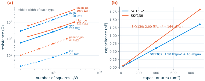
For SG13G2 the extraction returns exactly the specification’s targets: 7.0, 260 and 1360 Ω/□, end resistances of 4.6, 35 and 77 Ω·µm (specified 4.5, 35 and 80), and 1.50 fF/µm² plus 40 aF/µm for the MIM capacitor [15]. For SKY130 we find 48 Ω/□ for the generic poly resistor (documented 48.2), 320 Ω/□ for res_high_po (about 300; fitted over all five of its characterized widths, see Chapter 25) and 1998 Ω/□ for res_xhigh_po (2000), and 2.00 fF/µm² for the MIM capacitor (2 fF/µm²) [18]. The SKY130 precision resistors also have a large end resistance, about 140–160 Ω·µm per end on average (it changes with the width, which Chapter 25 follows width by width), and the effective width of res_high_po is about 0.04 µm narrower than drawn.
Worked example 3.1 · A 10 kΩ resistor in each PDK
SG13G2,
\[L = \left(R - \frac{2R_c}{W}\right)\frac{W+\Delta W}{R_\square} = (10\,000 - 70)\,\frac{1.006}{260} = 38.42\ \mu\mathrm{m}.\]rppd, W = 1 µm. Solve Eq. (3.2) for L with the specification values \(R_\square\) = 260 Ω/□, \(\Delta W\) = 6 nm and \(R_c\) = 35 Ω·µm:The simulated resistor measures 10.00 kΩ.
SKY130,
res_high_po_0p69(W = 0.69 µm). With only the documented 300 Ω/□, the obvious answer is \(L = 10\,000 \cdot 0.69/300 = 23.0\) µm. The simulation gives 11.70 kΩ, 17 % too high: the real sheet resistance adds 7 %, the narrower effective width 6 % and the two ends another 4 %. With the extracted values (320 Ω/□, \(W + \Delta W\) = 0.65 µm, \(R_c\) = 157 Ω·µm), Eq. (3.2) gives L = 19.40 µm, and the simulation 9.93 kΩ, within 1 %.The lesson: for a resistor whose absolute value matters, use all three terms of Eq. (3.2), or simply simulate a single resistor and scale its length.
What this means for your design
- Headroom, not current, is SG13G2’s constraint. Its core transistors are as strong as SKY130’s per micrometre, but every stack of transistors must fit into 1.2 V. Expect fewer cascodes and more careful bias design than in SKY130, while the intrinsic gain (Chapter 6) pushes you towards cascodes at the same time. That tension is the central design problem of the SG13G2 course project.
- Large resistors are cheaper in SG13G2.
rhigh(1360 Ω/□) and the SKY130res_xhigh_po(2000 Ω/□) are comparable, but SG13G2’s resistors can be drawn at any width, which makes ratio-matched layouts easier.- Capacitors are slightly denser in SKY130 (2.0 against 1.5 fF/µm²): a 2 pF MIM capacitor, the size of the course project’s load, occupies 1000 µm² in SKY130 and 1330 µm² in SG13G2.
3.5 Models, corners and how the simulator finds them
A netlist names a device, for example sg13_lv_nmos; the simulator must find what that name means. In both PDKs the answer is a chain of files, shown in Figure 3.4.
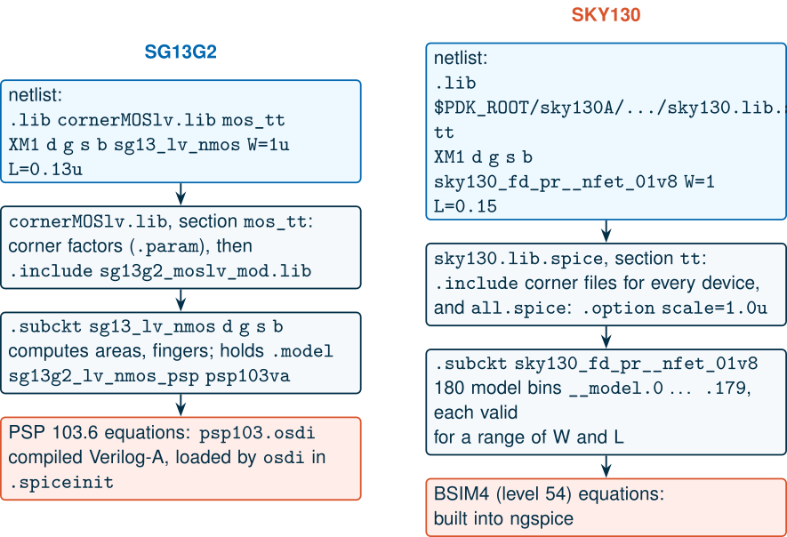
.lib statement selects a corner section, which sets corner parameters and includes the model files; the transistor is a subcircuit around a compact model. SG13G2's PSP equations come from a compiled Verilog-A library loaded through OSDI; SKY130's BSIM4 is built into ngspice.The .lib statement. A model library is one file with several named sections, each between .lib name and .endl name. Writing .lib file section in a netlist reads just that section. For transistors, the sections are the process corners: tt (typical NMOS, typical PMOS), ff, ss, fs and sf, which shift the model parameters to bracket the spread of production wafers. Each PDK splits its devices into several libraries.
Table 3.4. Where the models are, in IIC-OSIC-TOOLS ($PDK_ROOT = /foss/pdks).
| Quantity | SG13G2 | SKY130 |
|---|---|---|
| Model folder | $PDK_ROOT/ihp-sg13g2/libs.tech/ngspice/models |
$PDK_ROOT/sky130A/libs.tech/ngspice (binned) and .../libs.tech/combined (continuous) |
| Core MOSFETs | .lib cornerMOSlv.lib mos_tt |
.lib .../sky130.lib.spice tt (one file for all devices) |
| Other devices | cornerMOShv.lib mos_tt, cornerHBT.lib hbt_typ, cornerRES.lib res_typ, cornerCAP.lib cap_typ, cornerDIO.lib dio_tt |
in the same tt section |
| Corners | mos_tt, mos_ff, mos_ss, mos_fs, mos_sf; res_bcs, res_wcs, … |
tt, ff, ss, fs, sf, plus resistor/capacitor combinations such as ss_hh |
| Mismatch and Monte Carlo | mos_tt_mismatch, mos_tt_stat |
tt_mm, mc |
| Model equations | PSP 103.6, osdi/psp103.osdi |
BSIM4 4.5, built in |
| Units of W and L | metres: W=1u L=0.13u |
micrometres: W=1 L=0.15 (.option scale=1.0u) |
How the files are found. IIC-OSIC-TOOLS sets the variable SPICE_USERINIT_DIR to the active PDK’s libs.tech/ngspice folder, and ngspice reads the .spiceinit file there at start-up. For SG13G2 that file does two things: it adds the model folder to ngspice’s search path, which is why a bare .lib cornerMOSlv.lib mos_tt works from any directory, and it loads the compiled models with osdi commands (psp103.osdi, r3_cmc.osdi for the resistors, mosvar.osdi for the varactor and others). For SKY130 the .lib statement carries the full path, and the start-up file only sets compatibility options. Chapter 2 shows what happens when either step is missing.
The scale option. The SKY130 library contains .option scale=1.0u, which multiplies every length on an instance line by 10⁻⁶. In SKY130 you therefore write W=1 L=0.15, and W=1u would mean a width of 10⁻¹² m. SG13G2 does not use the option, so its instances take SI units. Mixing the two conventions is the most common error in this course; Section 2.6 shows its symptoms.
SG13G2 vs SKY130 · Two model libraries in SKY130
The SKY130 installation has two model sets, each with the same corner sections:
- Binned:
libs.tech/ngspice/sky130.lib.spice, the original models. Each transistor type is a set of model bins (180 fornfet_01v8), each fitted for a small range of W and L.- Combined:
libs.tech/combined/sky130.lib.spice, re-characterized continuous models whose parameters vary smoothly with W and L, plus the original models for the devices that were not refitted [20, 19].Xschem’s SKY130
cornersymbol in IIC-OSIC-TOOLS uses the combined set (the testbenches of Chapter 2 therefore do too). All other SKY130 numbers in this book, including Table 3.3 and the lookup tables of Chapter 6, come from the binned set. At the widths where the original models were fitted (1, 3, 4, 5 µm and others) the two agree to better than 1 %. Between them they can differ: for an NMOS with L = 0.18 µm and \(V_{GS} = V_{DS}\) = 0.9 V, we simulated 42.3 µA/µm at W = 2 µm with the binned set and 33.5 µA/µm with the continuous one. With either set, ngspice must run withset ngbehavior=hsa(IIC-OSIC-TOOLS sets it in~/.spiceinit) so that a device with several fingers is matched to the bin of its finger width W/nf; without it, our 10 µm wide, two-finger NMOS was binned on its total width and its on-current came out 7 % low. SG13G2’s PSP model is continuous in W and L by construction.
Corners
Figure 3.5 shows how far the corners move the on-current of the core devices.
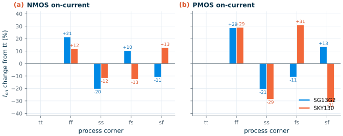
In SG13G2 the corners act symmetrically on both devices: ff raises the NMOS on-current by 21 % and ss lowers it by 20 %, with thresholds of 0.437 V and 0.552 V against 0.500 V at tt. In SKY130 the NMOS moves by only ±12 %, the PMOS by +29 % and −29 %.
Common pitfall · Assuming the letters of a skewed corner mean the same thing in every PDK
In SG13G2 the first letter of
mos_fsrefers to the NMOS: our simulation gives a faster NMOS (+10 %) and a slower PMOS (−11 %). In SKY130 the comment at the top ofsky130.lib.spicedescribesfsthe same way, as “Fast N / Slow P”, but the models do the opposite: atfsthe NMOS on-current falls by 13 % and the PMOS current rises by 31 %, andsfis the mirror image. We checked this with both SKY130 libraries in the container. Before you sign off a design over corners, simulate one transistor of each type at each corner and write down what each corner really does.
3.6 Design rules at a glance
Design rules are the geometric limits that keep a layout manufacturable: minimum widths of each layer, minimum spacings between shapes, how far one layer must enclose another (a contact inside its diffusion), and how far a layer must extend past another (the gate poly beyond the end of the channel). The SG13G2 rule document alone runs to 75 pages [16, 18]; the DRC decks in each PDK check all of them automatically (Chapter 16). Figure 3.6 shows the handful that shape every transistor you will draw, and Table 3.5 gives their values.
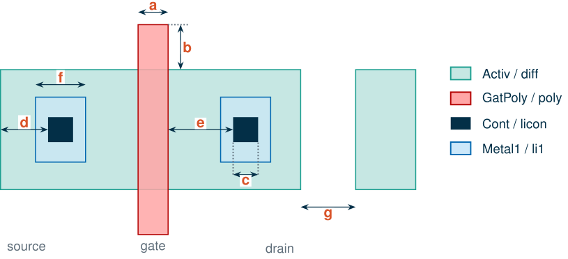
Table 3.5. Key layout rules in µm [16, 18]. Rule names in brackets.
| Rule | SG13G2 | SKY130 |
|---|---|---|
| a · minimum gate length (poly width) | 0.13 (Gat.a) | 0.15 (poly.1a) |
| b · poly extension beyond diffusion (end cap) | 0.18 (Gat.c) | 0.13 (poly.8) |
| c · contact size | 0.16 (Cnt.a) | 0.17 (licon.1) |
| d · diffusion enclosure of contact | 0.07 (Cnt.c) | 0.04 (licon.5a) |
| e · contact to gate spacing | 0.11 (Cnt.f) | 0.055 (licon.11) |
| f · minimum width of first wiring layer | 0.16 Metal1 (M1.a) | 0.17 li1 (li.1), 0.14 met1 (m1.1) |
| g · diffusion to diffusion spacing | 0.21 (Act.b) | 0.27 (difftap.3) |
| poly to poly spacing | 0.18 (Gat.b) | 0.21 (poly.2) |
| first-metal spacing | 0.18 (M1.b) | 0.17 li1 (li.3), 0.14 met1 (m1.2) |
| minimum width of TopMetal1 / met5 | 1.64 (TM1.a) | 1.6 (m5.1) |
You will rarely apply these numbers by hand, because the PDK’s parametrized cells draw every device correctly and the DRC catches the rest. But they explain sizes you will see: for example, the smallest SG13G2 transistor’s source region must hold a 0.16 µm contact, 0.11 µm from the gate and 0.07 µm inside the diffusion, so it extends at least 0.34 µm from the gate. That is where the default source and drain areas of the device models come from, and why a transistor’s drain capacitance does not shrink below a certain size.
Try it · Lab 1
In Lab 1 you characterize the core NMOS and PMOS of your chosen PDK: draw the testbench of Chapter 2, extract the threshold voltage with Eq. (3.1), the on- and off-currents and the subthreshold slope, and compare them with Table 3.3. Then repeat at the
ssandffcorners and at −40 °C and 125 °C.
- Both PDKs are 130 nm processes with the same front end (STI, wells, poly gates, salicide) but different back ends: SG13G2 has five thin and two thick aluminium metals and a SiGe HBT; SKY130 has a local interconnect and five metals.
- The core transistors have similar on-currents per micrometre (479 and 529 µA/µm for the NMOS), but SG13G2 delivers it from 1.2 V with a 0.50 V threshold, SKY130 from 1.8 V with a 0.72 V threshold.
- Passive devices follow Eq. (3.2) for resistors and an area-plus-perimeter law for capacitors; the models reproduce the documented values, but the SKY130 precision resistors need their width bias and end resistance to be sized accurately.
- A
.lib file sectionstatement selects the corner; SG13G2’s PSP model is loaded as a compiled OSDI library by.spiceinit; SKY130 lengths are in micrometres because of.option scale=1.0u.- SKY130 ships binned and continuous model libraries, and its skewed corners act opposite to their names; check both before you trust a corner run.
- Design rules set the minimum geometry of every device; you rarely apply them by hand, but they explain device sizes and parasitics.
Further reading
- IHP, SG13G2 Process Specification [15] and Layout Rules [16]: short, readable documents with every number in this chapter’s SG13G2 column.
- SkyWater, SKY130 PDK documentation [18]: device details, the process stack and the full rule set.
- G. Gildenblat et al. [73]: the PSP model behind SG13G2’s transistors.
- Y. Tsividis and C. McAndrew [58]: how compact models such as BSIM4 and PSP describe a MOSFET.
- The PDK Devices in 3D gallery of this site.