Chapter 10
The Differential Pair and the 5T OTA
Two matched transistors sharing a tail current reject everything their inputs have in common. Add a current-mirror load and you have the five-transistor OTA, the simplest complete amplifier.
- Explain why differential signalling rejects common-mode noise.
- Derive the large- and small-signal behaviour of the differential pair, and relate its linear range to gm/ID.
- Analyse the five-transistor OTA: gain, mirror pole-zero doublet, CMRR, input range, output swing and slew rate.
- Design a 5T OTA with gm/ID for the course load in both PDKs and verify it as a unity-gain buffer.
- Explain why a single stage cannot meet the course’s 60 dB gain specification.
Contents
10.1 Why differential?
The amplifiers of Chapters 7 and 9 amplify a voltage measured against ground. On a chip, “ground” and the supply are not quiet: digital switching, substrate currents and the bond-wire inductance move them by tens of millivolts. A single-ended amplifier cannot tell such disturbances from the signal.
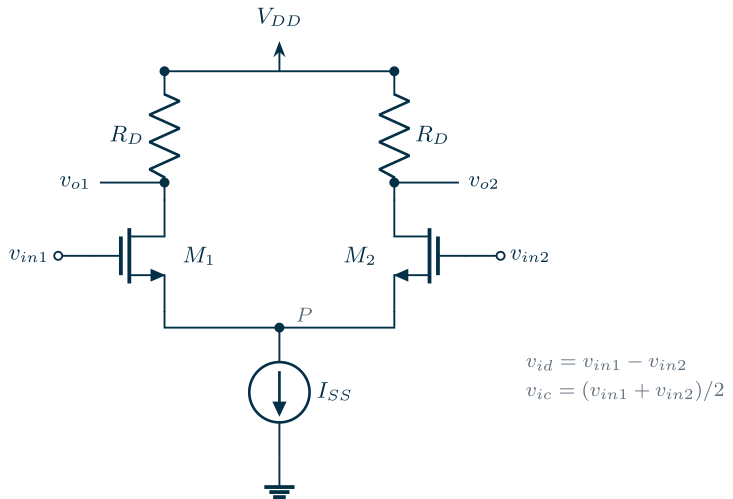
A differential circuit processes the difference between two voltages. Any two inputs \(v_{in1}\) and \(v_{in2}\) can be split into a differential-mode part and a common-mode part,
\[v_{id} = v_{in1} - v_{in2}, \qquad v_{ic} = \frac{v_{in1} + v_{in2}}{2}, \qquad v_{in1,2} = v_{ic} \pm \frac{v_{id}}{2}. \tag{10.1}\]If both inputs are routed side by side, a disturbance couples into both equally and appears only in \(v_{ic}\). A circuit that responds to \(v_{id}\) and ignores \(v_{ic}\) therefore rejects it. Differential signalling has further benefits: the output swing doubles for the same supply, even-order distortion cancels by symmetry, and the bias point no longer depends on an accurate reference for “zero”.
The circuit that does this is the differential pair of Figure 10.1: two matched transistors whose sources are tied together and fed by a tail current \(I_{SS}\). The tail is the key. Because \(I_{D1} + I_{D2} = I_{SS}\) is fixed, a common-mode input that raises both gates can only raise the shared source node P; the currents, and hence the outputs, stay put. A differential input, on the other hand, steers current from one side to the other.
10.2 Large-signal behaviour
How much differential input does it take to steer all of \(I_{SS}\) into one transistor? The answer depends on the inversion level, and gm/ID is the natural way to express it.
In strong inversion each transistor follows the square law, \(I_D = \tfrac12 k (V_{GS} - V_{TH})^2\) with \(k = \mu C_{ox}W/L\). Writing \(\Delta V = v_{id}\) and eliminating the source voltage gives the classic result [51, 53]
\[\Delta I_D = I_{D1} - I_{D2} = \tfrac12 k\,\Delta V\sqrt{\frac{4I_{SS}}{k} - \Delta V^2}, \qquad \lvert\Delta V\rvert \le \sqrt2\,V_{OV}, \tag{10.2}\]where \(V_{OV}\) is the overdrive of each device at balance. Beyond \(\sqrt2\,V_{OV}\) one transistor is off.
In weak inversion each current is exponential in its gate-source voltage, \(I_D \propto \exp(V_{GS}/nU_T)\), and the ratio of the two currents depends only on \(\Delta V\):
\[\frac{\Delta I_D}{I_{SS}} = \tanh\frac{\Delta V}{2nU_T}. \tag{10.3}\]Both results collapse onto one picture if we use the variable \(x = \Delta V\cdot(g_m/I_D)/2\), where \(g_m/I_D\) is that of each transistor at balance. Then \(\Delta I_D/I_{SS} = \tanh x\) in weak inversion and \(x\sqrt{1 - x^2/4}\) in strong inversion (since \(g_m/I_D = 1/nU_T\) and \(2/V_{OV}\) in the two limits). Define the linear range \(V_{lin}\) as the differential input at which the large-signal transconductance \(\Delta I_D/\Delta V\) has fallen 10 % below its small-signal value \(g_m\). Solving \(\tanh x/x = 0.9\) and \(\sqrt{1 - x^2/4} = 0.9\):
Key equation · Linear range of the differential pair
\[\frac{1.13}{g_m/I_D} \;\le\; V_{lin} \;\le\; \frac{1.74}{g_m/I_D}, \tag{10.4}\]from weak inversion (left) to the square law (right). The linear range is inversely proportional to gm/ID: an efficient, low-power pair is also a nonlinear one.
Simulation in both PDKs
Figure 10.2 checks Eq. (10.4) with eight pairs of 5 µm by 1 µm transistors per PDK, each biased by its own ideal tail current so that its gm/ID at balance runs from 4 to 24 V⁻¹. The bulk of each pair is tied to its sources here, so that the devices behave exactly like the table. The simulated linear range falls from 416 mV (SG13G2) and 454 mV (SKY130) at gm/ID = 4 to 56 mV and 52 mV at gm/ID = 24, and it stays between the two limits of Eq. (10.4) across moderate inversion. At gm/ID = 4 the SKY130 pair is slightly more linear than the square law predicts (454 against 436 mV), because velocity saturation and mobility degradation flatten the current at high overdrive.
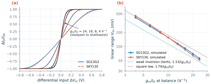
The two PDKs land on almost the same curves, even though their threshold voltages differ by 0.3 V. That is the gm/ID idea of Chapter 6 once more: the inversion level, not the gate voltage, sets the behaviour.
What this means for your design
In an OTA used in a feedback loop, the input pair only sees the small error voltage, so nonlinearity is rarely the limit; choose a high gm/ID (15–20 V⁻¹) for efficiency and low noise. When the pair must handle large differential signals without feedback, as in a transconductor or the input of a comparator’s preamplifier, drop gm/ID: a pair at gm/ID = 8 stays within 10 % of linear up to about 200 mV in both PDKs. The slew rate in Section 10.7 is the other face of the same coin: once \(\lvert v_{id}\rvert\) exceeds a few \(V_{lin}\), the pair simply switches all of \(I_{SS}\).
10.3 Small-signal gain
For small inputs the pair is linear, and symmetry makes its analysis easy. Apply a purely differential input, \(v_{in1} = +v_{id}/2\) and \(v_{in2} = -v_{id}/2\). One transistor’s current rises by \(g_m v_{id}/2\) and the other’s falls by the same amount, so the tail current, and therefore the voltage of node P, does not change. For differential signals P is a virtual AC ground, and each side behaves like a common-source stage driven by \(\pm v_{id}/2\). This is the half-circuit [51, 53]. With load resistors \(R_D\) and \(R_o = R_D \parallel r_o\):
\[A_{dm} = \frac{v_{o1} - v_{o2}}{v_{id}} = -g_m R_o. \tag{10.5}\]For a common-mode input both currents move together, and P moves with the inputs. The tail source has a finite output resistance \(R_{SS}\) (for a transistor, its \(r_o\)), so each half sees a degeneration resistance of \(2R_{SS}\) (the halves share \(R_{SS}\), each carrying half its current) and
\[A_{cm} = \frac{v_{o1}}{v_{ic}} = -\frac{R_o}{1/g_m + 2R_{SS}} \approx -\frac{R_o}{2R_{SS}}. \tag{10.6}\]With perfectly matched halves, the differential output \(v_{o1} - v_{o2}\) contains no common-mode signal at all; the single-ended outputs contain a little, suppressed by the ratio \(2R_{SS}/R_o\).
10.4 Common-mode rejection
The figure of merit is the common-mode rejection ratio, the ratio of the wanted to the unwanted gain:
\[\mathrm{CMRR} = \left\lvert\frac{A_{dm}}{A_{cm}}\right\rvert. \tag{10.7}\]For the single-ended output of the resistively loaded pair, Eqs. (10.5) and (10.6) give \(\mathrm{CMRR} \approx 2g_m R_{SS}\): a good tail source is everything. Three things spoil CMRR in practice.
- Mismatch. If the two halves differ, a common-mode input produces a differential output. Random mismatch is the subject of Chapter 13; here we look at systematic effects only.
- Asymmetric bias. If the two transistors sit at different drain voltages they have different \(g_{ds}\), and the halves are no longer identical even with perfect layout. Section 10.5 shows that this dominates in the 5T OTA.
- Frequency. The tail node has capacitance (the tail transistor’s drain and the pair’s sources), so \(R_{SS}\) is shunted at high frequency and CMRR falls.
10.5 The five-transistor OTA
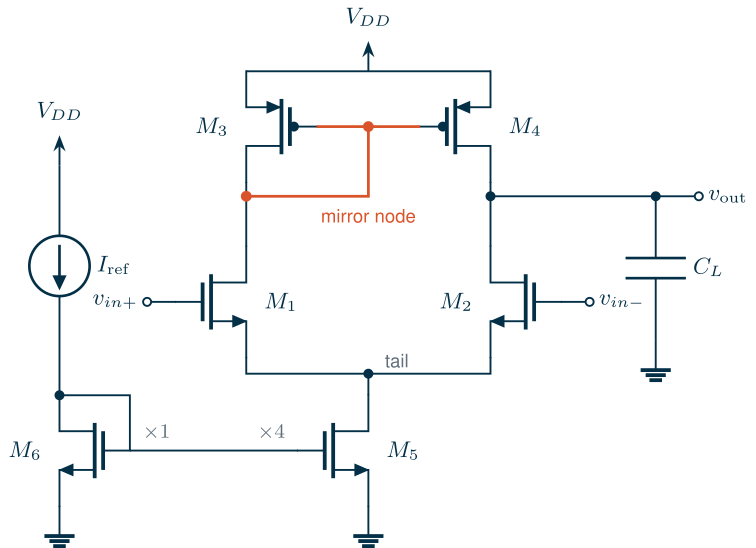
Replace the two load resistors by a PMOS current mirror and take the output from one side: Figure 10.3 is the five-transistor operational transconductance amplifier (5T OTA). The mirror converts the differential output current to a single-ended one. When \(v_{in+}\) rises, \(M_1\) takes more of the tail current; the diode \(M_3\) passes this increase to \(M_4\), which pushes it into the output, while \(M_2\) takes less and pulls less out. Both effects raise the output, so the full differential current \(g_{m1}v_{id}\) reaches the output, not just half of it. Note the polarity: the input on the diode side is the non-inverting one.
Throughout this section we use the OTA designed in Section 10.8; its device sizes are in Table 10.1.
Gain and bandwidth
The output resistance is that of \(M_2\) and \(M_4\) in parallel, so
Key equation · Gain and gain-bandwidth of the 5T OTA
\[A_0 = g_{m1}\left(r_{o2} \parallel r_{o4}\right) = \frac{g_{m1}}{g_{ds2} + g_{ds4}}, \qquad \mathrm{GBW} = \frac{g_{m1}}{2\pi C_L}. \tag{10.8}\]\(C_L\) includes the drain capacitances of \(M_2\) and \(M_4\). The gain is about half the intrinsic gain of one transistor, independent of the current.
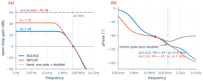
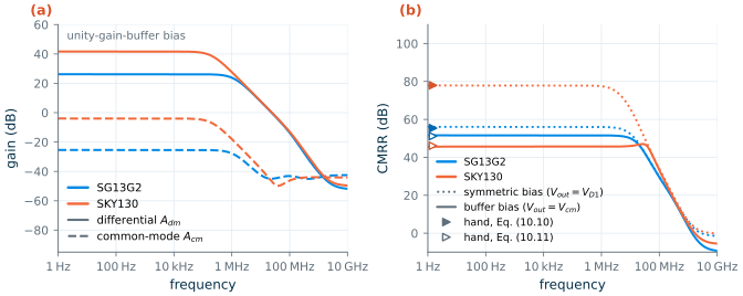
Equation (10.8) tells the whole story of this chapter’s design problem. The DC gain is limited to about \(\tfrac12 g_m/g_{ds}\), and from Chapter 6 we know that this is 13 to 20 in SG13G2 and 65 to 100 in SKY130 for lengths of 0.5 to 2 µm. Figure 10.4(a) shows the simulated open-loop response of the two designs: 26.2 dB in SG13G2 and 41.7 dB in SKY130, against hand predictions of 27.0 and 41.6 dB. Both cross 0 dB just above 20 MHz, as designed. Both are far below the 60 dB line.
The mirror pole-zero doublet
The signal of the left half travels through the mirror node, which has a resistance of about \(1/g_{m3}\) and the capacitance \(C_m\) of the gates of \(M_3\) and \(M_4\) plus the drains of \(M_1\) and \(M_3\). This path has a pole at \(\omega_m = g_{m3}/C_m\). The right half reaches the output directly, with no such pole. Half the signal is delayed and half is not, so the transfer function has a pole at \(\omega_m\) and a left-half-plane zero at \(2\omega_m\) [51, 52]:
\[\frac{v_{out}}{v_{id}} \approx A_0\,\frac{1 + s/(2\omega_m)}{\left(1 + s/\omega_{p1}\right)\left(1 + s/\omega_m\right)}, \qquad \omega_{p1} = \frac{1}{(r_{o2}\parallel r_{o4})\,C_L}, \quad \omega_m = \frac{g_{m3}}{C_m}. \tag{10.9}\]A closely spaced pole and zero like this is called a doublet. Its phase dip, at most 19.5° at \(\sqrt2\,\omega_m\), matters only if it is near the unity-gain frequency. With the hand values (\(C_m\) = 266 fF and 202 fF, \(g_{m3}\) = 200 µS), the mirror pole is at 120 MHz in SG13G2 and 158 MHz in SKY130, five to six times the GBW, and Eq. (10.9) predicts phase margins of 84° and 85°. The simulation gives 87° and 85°, and its pole-zero analysis places the mirror poles at 149 MHz (SG13G2) and 186 MHz (SKY130), with the zeros about 2.4 times higher, at 352 and 440 MHz. The hand estimate of \(C_m\), summed from the table’s gate and drain capacitances, is 15–25 % larger than the simulated pole implies; because the doublet sits well above the GBW, this error moves the predicted phase margin by less than 3°.
Common pitfall · Swapping the inputs of a 5T OTA
The input on the diode side of the mirror (\(M_1\) in Figure 10.3) is the non-inverting input, because its signal is inverted twice: once by \(M_1\) and once more by the mirror. Connect the output back to the wrong input and the “buffer” latches to a rail. In Xschem, label the pins
inpandinnfrom this rule, not from the drawing’s symmetry.
Common-mode rejection of the OTA
With perfect symmetry, a common-mode input moves the mirror node and the output by the same amount, which is set by how much the tail current changes: \(v_{out} = v_{n1} \approx -v_{ic}/(2g_{m3}R_{SS})\). This gives the textbook result
\[\mathrm{CMRR}_\mathrm{sym} = A_0 \cdot 2g_{m3}R_{SS}, \tag{10.10}\]55.4 dB (SG13G2) and 78.0 dB (SKY130) for our designs, with \(R_{SS} = 1/g_{ds5}\). But the symmetry only holds if the output sits at the mirror-node voltage. In a unity-gain buffer the output sits at the input common-mode voltage instead (0.70 V and 1.10 V here, against 0.68 V and 0.63 V at the mirror node), so \(M_1\) and \(M_2\) have different drain-source voltages and different output conductances. The imbalance adds a common-mode gain of its own:
\[\lvert A_{cm}\rvert \approx \frac{1}{2g_{m3}R_{SS}} + \frac{\lvert g_{ds1} - g_{ds2}\rvert}{g_{ds2} + g_{ds4}}. \tag{10.11}\]In SKY130 the second term is 0.58 (the 0.47 V higher output gives \(M_2\) about half the \(g_{ds}\) of \(M_1\)), forty times the first, and the predicted CMRR drops to 46.1 dB. Figure 10.5 confirms both cases: the simulated CMRR is 56.1 dB and 77.9 dB with symmetric bias, and 51.6 dB and 45.6 dB in the buffer, within 0.5 dB of Eqs. (10.10) and (10.11). Above a few megahertz the tail and mirror capacitances take over and the CMRR falls in every case.
The same imbalance produces a systematic offset: to hold the output 0.47 V away from the mirror node, the SKY130 OTA needs a differential input of about \(0.47\,\mathrm{V}/121 = 3.9\) mV. The simulated buffer error is −4.3 mV (SKY130) and −1.1 mV (SG13G2). Like the CMRR loss, this is a property of the topology, not of mismatch.
10.6 Input and output range
A transistor amplifies only while it is saturated, which in moderate inversion means \(V_{DS} \ge V_{DS,sat}\), with \(V_{DS,sat}\) read from the table (it is about 3–5 \(U_T\) in weak inversion and approaches \(V_{OV}\) in strong inversion). Applying this to \(M_5\) and \(M_1\) gives the input common-mode range (ICMR):
Key equation · Input common-mode range and output swing of the 5T OTA
\[V_{GS1} + V_{DS,sat5} \;\le\; V_{ic} \;\le\; V_{DD} - \lvert V_{GS3}\rvert + V_{GS1} - V_{DS,sat1}, \tag{10.12}\] \[V_{ic} - V_{GS1} + V_{DS,sat1} \;\le\; V_{out} \;\le\; V_{DD} - \lvert V_{DS,sat4}\rvert. \tag{10.13}\]\(V_{GS1}\) includes the body effect, because the pair’s sources sit above ground; we estimate it with \(\partial V_{TH}/\partial V_{SB} \approx g_{mb}/g_m\) from the tables.
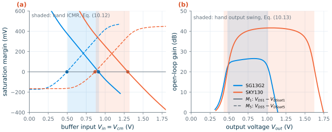
The upper limit of Eq. (10.12) is set by the PMOS load: the mirror node sits \(\lvert V_{GS3}\rvert\) below the supply, and \(M_1\) needs \(V_{DS,sat1}\) below that. The lower limit is set by the tail. With the table values (SG13G2: \(V_{GS1}\) = 0.36 V, \(\lvert V_{GS3}\rvert\) = 0.52 V; SKY130: 0.77 V and 1.17 V), the predicted ICMR is 0.51–0.92 V in SG13G2 and 0.88–1.32 V in SKY130. The output swing in a buffer is the same range, since \(V_{out} = V_{in}\).
Figure 10.6(a) checks it by sweeping the input of the unity-gain buffer and watching the saturation margins \(V_{DS} - V_{DS,sat}\) of \(M_5\) and \(M_1\) in the simulator. Both stay positive from 0.50 to 0.91 V in SG13G2 and from 0.87 to 1.30 V in SKY130, within 25 mV of the hand values. Panel (b) shows the open-loop gain against the output voltage, with the input common-mode voltage fixed: the gain stays within 6 dB of its peak from 0.47 to 1.02 V and from 0.59 to 1.52 V. The hand limits of Eq. (10.13) are 0.48–1.01 V and 0.43–1.62 V. The high-gain SKY130 stage loses half its gain about 100 mV before its transistors formally leave saturation, because its gain depends on very small output conductances, which start to rise early.
SG13G2 vs SKY130 · What 0.6 V of extra supply buys
SKY130 has 50 % more supply, yet its simulated ICMR is barely wider (0.43 V against 0.42 V) and occupies a smaller fraction of the supply (24 % against 35 %). The higher supply is spent on higher thresholds: the SKY130 input pair needs 0.77 V of gate-source voltage (including 0.10 V of body effect) and its PMOS load 1.17 V, against 0.36 V and 0.52 V in SG13G2 (Chapter 6 showed the thresholds). Neither range includes mid-supply comfortably, and neither includes 0.2 V or \(V_{DD} - 0.2\) V, the course’s output-swing specification. Rail-to-rail swing will need a second stage (Chapter 12).
10.7 Slew rate
For large input steps the pair switches completely (Section 10.2), and the whole tail current flows into or out of the load capacitor. The output can then change no faster than
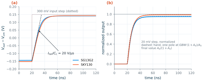
\[\mathrm{SR} = \frac{I_{tail}}{C_L}, \tag{10.14}\]independent of the gain or bandwidth. A unity-gain buffer with \(\mathrm{GBW} = \omega_u/2\pi\) responds to a small step exponentially with time constant \(1/\omega_u\), so its initial slope is \(V_{step}\,\omega_u\). It slews whenever that slope would exceed SR, that is for steps larger than \(\mathrm{SR}/\omega_u\) = 20 V/µs ÷ (2π · 24 MHz) ≈ 0.13 V here.
Figure 10.7(a) shows the response of both buffers to a 300 mV step, the largest that fits comfortably in the SG13G2 input range. The output first ramps linearly at a slope close to \(I_{tail}/C_L\) = 20 V/µs: the simulated maximum slopes are 20.4 V/µs rising and 17.7 V/µs falling in SG13G2, and 19.4 and 21.9 V/µs in SKY130. Then it settles exponentially. The rising and falling slopes differ by up to 20 % because the tail current itself changes while the tail node moves with the input. For a 20 mV step (panel b) there is no slewing: the response is the first-order exponential predicted from the GBW, settling to \(A_0/(1 + A_0)\) of the step (95 % in SG13G2, 99 % in SKY130). The missing 5 % is the gain error of a 26 dB amplifier in unity feedback.
10.8 Designing a 5T OTA in both PDKs
We now design the OTA used above for the course load: \(C_L\) = 2 pF, GBW ≥ 20 MHz, slew rate ≥ 10 V/µs, biased from a 10 µA reference, at 1.2 V (SG13G2) and 1.8 V (SKY130). The procedure follows the gm/ID recipe of Section 6.5 [56], with one decision per transistor role.
Worked example 10.1 · Sizing the 5T OTA with gm/ID
1. Input transconductance. Allow 25 % margin for parasitic capacitance and the doublet: \(g_{m1} = 2\pi \cdot 25\ \mathrm{MHz} \cdot 2\ \mathrm{pF} = 314\ \mu\mathrm{S}\).
2. Tail current. The slew rate needs \(I_{tail} \ge 10\ \mathrm{V/\mu s} \cdot 2\ \mathrm{pF} = 20\) µA. A 1:4 mirror from the 10 µA reference gives \(I_{tail}\) = 40 µA (SR = 20 V/µs), so each input device carries 20 µA.
3. Input pair. \(g_{m1}/I_D = 314/20 = 15.7\); round to 16 V⁻¹ (moderate inversion, efficient and low-noise), so \(g_{m1}\) = 320 µS. Choose L = 1 µm: shorter lengths lose gain, longer ones add input capacitance for little gain (Figure 6.8). The width chart then gives the widths in Table 10.1.
4. Mirror load. \(g_m/I_D\) = 10 V⁻¹ (strong side of moderate inversion, for matching and a high mirror pole). L = 1 µm keeps the mirror pole above 5 × GBW; L = 2 µm would add less than 1 dB of gain but drop the pole to about 33 MHz (SG13G2) and 42 MHz (SKY130), too close to the GBW.
5. Tail and bias. L = 2 µm for a high \(R_{SS}\). The bias diode \(M_6\) is one 5 µm unit carrying 10 µA, and \(M_5\) is four such units: this fixes \(g_m/I_D\) = 11.3 (SG13G2) and 10.8 V⁻¹ (SKY130), with \(V_{DS,sat5} \approx\) 0.17 V.
6. Common-mode level. Eq. (10.12) gives the ICMR; we bias the buffer near its centre, at 0.70 V (SG13G2) and 1.10 V (SKY130).
7. Predict. Read \(g_{ds}\) and capacitances at each device’s actual \(V_{DS}\) and evaluate Eqs. (10.8)–(10.14). Every device is built from parallel units close to the 5 µm table width.
Table 10.1. Hand design of the 5T OTA (L in µm, W as units × unit width).
| Device | Role | gm/ID (V⁻¹) | L | W, SG13G2 | W, SKY130 | \(\lvert V_{GS}\rvert\), SG13G2 / SKY130 |
|---|---|---|---|---|---|---|
| M1, M2 | input pair, 20 µA each | 16 | 1 | 3 × 4.56 µm | 3 × 5.47 µm | 0.36 / 0.77 V (with body effect) |
| M3, M4 | mirror load | 10 | 1 | 3 × 4.95 µm | 3 × 5.76 µm | 0.52 / 1.17 V |
| M5 | tail, 40 µA | 11.3 / 10.8 | 2 | 4 × 5 µm | 4 × 5 µm | 0.36 / 0.73 V |
| M6 | bias diode, 10 µA | 11.3 / 10.8 | 2 | 1 × 5 µm | 1 × 5 µm | 0.36 / 0.73 V |
Table 10.2. Predicted and simulated performance (tt, 27 °C, unity-gain buffer at Vic, CL = 2 pF).
| Quantity | Spec | SG13G2 hand | SG13G2 sim | SKY130 hand | SKY130 sim |
|---|---|---|---|---|---|
| DC gain | ≥ 60 dB | 27.0 dB | 26.2 dB | 41.6 dB | 41.7 dB |
| GBW | ≥ 20 MHz | 25.1 MHz | 23.8 MHz | 25.2 MHz | 24.5 MHz |
| Phase margin (buffer) | ≥ 60° | 84° | 87° | 85° | 85° |
| Mirror pole / zero | 120 / 239 MHz | 149 / 352 MHz | 158 / 316 MHz | 186 / 440 MHz | |
| Slew rate (rise / fall) | ≥ 10 V/µs | 20 V/µs | 20.4 / 17.7 V/µs | 20 V/µs | 19.4 / 21.9 V/µs |
| CMRR, buffer bias | 51.2 dB | 51.6 dB | 46.1 dB | 45.6 dB | |
| ICMR | 0.51–0.92 V | 0.50–0.91 V | 0.88–1.32 V | 0.87–1.30 V | |
| Output swing (−6 dB gain) | 0.2 to \(V_{DD}\) − 0.2 V | 0.48–1.01 V | 0.47–1.02 V | 0.43–1.62 V | 0.59–1.52 V |
| Systematic offset | −1.1 mV | −4.3 mV | |||
| Power (incl. 10 µA reference) | low | 60 µW | 59.7 µW | 90 µW | 87.9 µW |
The hand design predicted every quantity that depends on transconductance and current (GBW, phase margin, slew rate) to within 5 %, and the gain to within 1 dB. Both designs meet the bandwidth, phase-margin and slew-rate targets with ease, at 60 µW and 88 µW. Both fail the gain specification, by 33.8 dB in SG13G2 and 18.3 dB in SKY130, and both fail the output-swing specification.
What this means for your design: why the course OTA needs two stages
Equation (10.8) says the 5T OTA’s gain is about half the intrinsic gain of one transistor. To reach 60 dB (1000) every transistor would need \(g_m/g_{ds} \approx 2000\), about 80 times what SG13G2 offers at L = 1 µm. Longer channels help slowly: with L = 2 µm for both the pair and the load, the hand estimate rises only to 29 dB in SG13G2 and 43 dB in SKY130, while the mirror pole drops below 40 MHz. Cascoding the output (a telescopic OTA) multiplies the gain by another \(g_m r_o\) but stacks two more saturation voltages into the supply, which leaves almost no swing at 1.2 V. The robust answer is a second gain stage: a common-source stage after the 5T OTA multiplies the gains and provides rail-to-rail output swing, at the price of a second pole that must be tamed with Miller compensation (Chapter 11). That is the two-stage OTA of Chapter 12, and this 5T OTA becomes its first stage.
Netlists
The two designs are stored as subcircuits, which Chapter 12 and Lab 5 reuse: tools/figs/ch10_ota5t_sg13g2.spice and tools/figs/ch10_ota5t_sky130.spice. The pins are vdd vss inp inn out ibias; sink the 10 µA reference into ibias. The testbench below measures the open-loop response of the unity-gain buffer: a 1 GH inductor closes the loop at DC so that the output sits at \(V_{ic}\), and a 1 F capacitor grounds the inverting input for every frequency above a millihertz [2].
* tools/figs/ch10_ota5t_sg13g2.spice (pins: vdd vss inp inn out ibias)
.subckt ota5t_sg13g2 vdd vss inp inn out ibias
XM1 n1 inp tail vss sg13_lv_nmos W=4.56u L=1u ng=1 m=3
XM2 out inn tail vss sg13_lv_nmos W=4.56u L=1u ng=1 m=3
XM3 n1 n1 vdd vdd sg13_lv_pmos W=4.95u L=1u ng=1 m=3
XM4 out n1 vdd vdd sg13_lv_pmos W=4.95u L=1u ng=1 m=3
XM5 tail ibias vss vss sg13_lv_nmos W=5u L=2u ng=1 m=4
XM6 ibias ibias vss vss sg13_lv_nmos W=5u L=2u ng=1 m=1
.ends ota5t_sg13g2
* open-loop AC of the unity-gain buffer
.include ch10_ota5t_sg13g2.spice
.lib cornerMOSlv.lib mos_tt
Vdd  vdd 0 1.2
Iref vdd ibias 10u
XOTA vdd 0 inp inn out ibias ota5t_sg13g2
CL   out 0 2p
Vin  inp 0 dc 0.7 ac 1
Lfb  out inn 1G            $ DC feedback: v(out) = v(inn) at DC
Cfb  inn 0 1               $ AC ground for the inverting input
.control
ac dec 50 1 10G
meas ac A0  find vdb(out) at=10
meas ac GBW when vdb(out)=0
meas ac PH  find vp(out) when vdb(out)=0
let PM = 180 + PH*180/pi
print PM
.endc
.end
* tools/figs/ch10_ota5t_sky130.spice (pins: vdd vss inp inn out ibias)
.subckt ota5t_sky130 vdd vss inp inn out ibias
XM1 n1 inp tail vss sky130_fd_pr__nfet_01v8 W=5.47 L=1 nf=1 ad='int((1+1)/2)*5.47*0.29' as='int((1+2)/2)*5.47*0.29' pd='2*int((1+1)/2)*(5.47+0.29)' ps='2*int((1+2)/2)*(5.47+0.29)' nrd=0 nrs=0 sa=0 sb=0 sd=0 mult=3 m=3
XM2 out inn tail vss sky130_fd_pr__nfet_01v8 W=5.47 L=1 nf=1 ad='int((1+1)/2)*5.47*0.29' as='int((1+2)/2)*5.47*0.29' pd='2*int((1+1)/2)*(5.47+0.29)' ps='2*int((1+2)/2)*(5.47+0.29)' nrd=0 nrs=0 sa=0 sb=0 sd=0 mult=3 m=3
XM3 n1 n1 vdd vdd sky130_fd_pr__pfet_01v8 W=5.76 L=1 nf=1 ad='int((1+1)/2)*5.76*0.29' as='int((1+2)/2)*5.76*0.29' pd='2*int((1+1)/2)*(5.76+0.29)' ps='2*int((1+2)/2)*(5.76+0.29)' nrd=0 nrs=0 sa=0 sb=0 sd=0 mult=3 m=3
XM4 out n1 vdd vdd sky130_fd_pr__pfet_01v8 W=5.76 L=1 nf=1 ad='int((1+1)/2)*5.76*0.29' as='int((1+2)/2)*5.76*0.29' pd='2*int((1+1)/2)*(5.76+0.29)' ps='2*int((1+2)/2)*(5.76+0.29)' nrd=0 nrs=0 sa=0 sb=0 sd=0 mult=3 m=3
XM5 tail ibias vss vss sky130_fd_pr__nfet_01v8 W=5 L=2 nf=1 ad='int((1+1)/2)*5*0.29' as='int((1+2)/2)*5*0.29' pd='2*int((1+1)/2)*(5+0.29)' ps='2*int((1+2)/2)*(5+0.29)' nrd=0 nrs=0 sa=0 sb=0 sd=0 mult=4 m=4
XM6 ibias ibias vss vss sky130_fd_pr__nfet_01v8 W=5 L=2 nf=1 ad='int((1+1)/2)*5*0.29' as='int((1+2)/2)*5*0.29' pd='2*int((1+1)/2)*(5+0.29)' ps='2*int((1+2)/2)*(5+0.29)' nrd=0 nrs=0 sa=0 sb=0 sd=0 mult=1 m=1
.ends ota5t_sky130
* open-loop AC of the unity-gain buffer
.include ch10_ota5t_sky130.spice
.lib "$PDK_ROOT/sky130A/libs.tech/ngspice/sky130.lib.spice" tt
Vdd  vdd 0 1.8
Iref vdd ibias 10u
XOTA vdd 0 inp inn out ibias ota5t_sky130
CL   out 0 2p
Vin  inp 0 dc 1.1 ac 1
Lfb  out inn 1G            $ DC feedback: v(out) = v(inn) at DC
Cfb  inn 0 1               $ AC ground for the inverting input
.control
ac dec 50 1 10G
meas ac A0  find vdb(out) at=10
meas ac GBW when vdb(out)=0
meas ac PH  find vp(out) when vdb(out)=0
let PM = 180 + PH*180/pi
print PM
.endc
.end
Try it · Lab 5
Lab 5 builds this OTA in Xschem for your PDK, checks the hand design of Table 10.1 with the testbench above, and measures the slew rate and ICMR. Then try L = 2 µm for the load and watch the gain rise by less than 1 dB while the phase margin falls, or move \(V_{ic}\) to mid-supply and find which transistor leaves saturation first.
- A differential pair steers a fixed tail current; common-mode inputs only move the shared source node, so they are rejected, and differential inputs see a virtual ground at that node.
- The linear range is set by gm/ID: between \(1.13/(g_m/I_D)\) in weak inversion and \(1.74/(g_m/I_D)\) for the square law, about 90 mV at gm/ID = 16 in both PDKs.
- The 5T OTA has \(A_0 = g_{m1}(r_{o2}\parallel r_{o4})\), about half the intrinsic gain, and GBW \(= g_{m1}/2\pi C_L\). Its mirror adds a pole at \(g_{m3}/C_m\) and a zero at twice that frequency.
- In a unity-gain buffer the output is not at the mirror-node voltage; the resulting \(g_{ds}\) imbalance limits the CMRR (46 dB in SKY130 instead of 78 dB) and creates a few millivolts of systematic offset.
- The ICMR follows from \(V_{DS,sat}\), not \(V_{GS} - V_{TH}\), in moderate inversion: 0.50–0.91 V in SG13G2 and 0.87–1.30 V in SKY130, about a third or a quarter of the supply.
- Designed with gm/ID for 2 pF and 20 MHz, the OTA meets GBW, phase margin and slew rate in both PDKs at 60–90 µW, but gives only 26 dB (SG13G2) and 42 dB (SKY130) of the 60 dB required: the two-stage OTA of Chapter 12 is needed.
Further reading
- B. Razavi, Design of Analog CMOS Integrated Circuits, Chapters 4 and 5 [51]: the differential pair, the active-load OTA and its common-mode behaviour.
- P. R. Gray, P. J. Hurst, S. H. Lewis and R. G. Meyer [53]: large-signal pair analysis in both bipolar and MOS forms, and CMRR with mismatch.
- P. G. A. Jespers and B. Murmann [56]: gm/ID-based design of OTAs, including the trade-offs of the input pair.
- H. Pretl et al., JKU analog circuit design course [2]: a 5T OTA designed and laid out in SG13G2, with notebooks.
- W. Sansen, Analog Design Essentials [62]: practical intuition for single-stage OTAs, CMRR and slew rate.