Chapter 14
Voltage References and Regulators
A bandgap reference adds a voltage that rises with temperature to one that falls with it, and the sum barely moves. A regulator then turns that reference into a clean supply. Both are built from the devices of the previous chapters plus the one bipolar transistor that every CMOS process gives you for free.
- Explain why bias circuits need a reference, and measure the temperature drift of the beta-multiplier of Chapter 8.
- Generate PTAT and CTAT voltages with the bipolar devices of SG13G2 and SKY130, and predict their slopes from the model parameters.
- Design a voltage-mode bandgap (SKY130, 1.8 V) and a current-mode bandgap that runs from 1.2 V (SG13G2), and simulate them from −40 °C to 125 °C.
- Explain start-up, curvature, trimming and the effect of real resistors.
- Design and simulate a simple low-dropout regulator, and check its loop stability and load regulation.
Contents
14.1 Why references?
Every analog block needs at least one quantity it can trust: the 10 µA bias current of our OTA, the full-scale voltage of an ADC, the output voltage of a regulator. The supply voltage is a poor candidate. It is set outside the chip, it varies from one board to the next by ±10 %, and it carries the noise of everything else on the chip. A reference is a circuit whose output depends on neither the supply nor, ideally, the temperature.
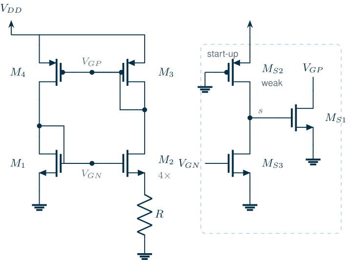
Chapter 8 took the first step with the beta-multiplier of Figure 14.1. Two NMOS transistors carry the same current, forced by the PMOS mirror, but \(M_2\) is four times wider, so it needs less gate-source voltage. The difference appears across \(R\):
\[I_{REF}\,R = V_{GS1} - V_{GS2}. \tag{14.1}\]The supply does not appear in Eq. (14.1), so the current is independent of \(V_{DD}\) to first order. We sized it with the gm/ID tables for 10 µA, \(M_1\) at \(g_m/I_D = 12\) and L = 2 µm, which gives \(R\) = 8.96 kΩ in SG13G2 and 7.32 kΩ in SKY130.
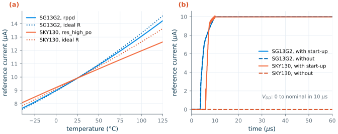
But Eq. (14.1) depends on temperature twice: the gate-voltage difference changes with mobility and threshold, and \(R\) has its own temperature coefficient. Figure 14.2a shows the result over the industrial range of −40 °C to 125 °C. With a PDK resistor the current changes by +66 % in SG13G2 (rppd) and +46 % in SKY130 (res_high_po); with an ideal, temperature-independent resistor the change is +71 % and +58 %: here the positive TC of these two resistors partly compensates the transistors. That is fine for biasing an amplifier, whose gm/ID design tolerates it, but useless as a measuring stick. We need a quantity that nature holds constant.
14.2 PTAT and CTAT voltages
The constant is the bandgap of silicon, and the device that reads it is the pn junction. The base-emitter voltage of a bipolar transistor at collector current \(I_C\) is
\[V_{BE} = V_T\ln\frac{I_C}{I_S}, \qquad I_S \propto T^{\,X_{TI}}\exp\!\left(-\frac{E_g}{kT}\right), \tag{14.2}\]where \(V_T = kT/q\) is the thermal voltage, \(E_g \approx 1.12\) eV the bandgap energy, and \(X_{TI}\) a fitting exponent of the saturation current (in textbooks \(4+m\), with \(m \approx -1.5\) from the mobility) [51, 53]. \(I_S\) grows so steeply with temperature that \(V_{BE}\) falls: differentiating at constant \(I_C\),
Key equation · The CTAT and PTAT voltages
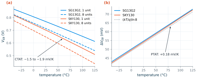
\[\frac{\partial V_{BE}}{\partial T} = \frac{V_{BE} - X_{TI}V_T - E_g/q}{T} \approx -1.5\ \text{to}\ -2\ \mathrm{mV/K}, \qquad \Delta V_{BE} = V_{BE1} - V_{BEN} = V_T\ln N. \tag{14.3}\]\(V_{BE}\) is complementary to absolute temperature (CTAT). The difference of the \(V_{BE}\) of two transistors at the same current but with emitter areas in the ratio \(N\) is proportional to absolute temperature (PTAT), with a slope of \((k/q)\ln N\), 0.179 mV/K for \(N = 8\). \(I_S\) and its uncertainty have cancelled.
Figure 14.3 shows both voltages for the substrate pnp transistors of the two PDKs at 2 µA. The SG13G2 device has \(V_{EB}\) = 0.769 V at 27 °C and a slope of −1.53 mV/K; the SKY130 device 0.701 V and −1.85 mV/K. Eq. (14.3) with each model’s own parameters (Table 14.1) predicts −1.56 and −1.84 mV/K, within 2 %. The PTAT differences are 54.7 mV and 54.1 mV at 27 °C, against \(V_T\ln 8\) = 53.8 mV, with slopes of +0.181 and +0.183 mV/K (theory +0.179 mV/K).
The idea of the bandgap reference follows at once: add the CTAT \(V_{BE}\) to a scaled PTAT \(\Delta V_{BE}\) so that their slopes cancel. Since \(\partial V_{BE}/\partial T \approx (V_{BE} - E_g/q)/T\), the sum that has zero slope is close to \(E_g/q\) plus a few \(V_T\), about 1.2 V: the bandgap voltage, hence the name.
14.3 Bipolar devices in SG13G2 and SKY130
A CMOS process has no dedicated bipolar transistor, but it always has a parasitic one. A p+ diffusion inside an n-well, above the p-type substrate, forms a vertical pnp: the p+ diffusion is the emitter, the n-well the base and the substrate the collector. Because the collector is the substrate, it is always tied to ground, so the transistor can only be used as a diode-connected device with base and collector grounded, exactly what a bandgap needs. Both PDKs model it; SG13G2, a BiCMOS process, also offers real SiGe npn transistors (Table 14.1). You can see these devices in the PDK Devices in 3D gallery.
Table 14.1. Bipolar devices for references, and their model parameters [14, 19].
| Quantity | SG13G2 | SKY130 |
|---|---|---|
| Substrate pnp | pnpMPA (subcircuit, any emitter W × L) |
sky130_fd_pr__pnp_05v5_W0p68L0p68, ..._W3p40L3p40 (two fixed emitters) |
| Instance | XQ1 c b e pnpMPA a=1.4e-12 p=5.4e-6 m=1 |
XQ1 c b e sky130_fd_pr__pnp_05v5_W3p40L3p40 m=1 mult=1 |
| Library section | .lib cornerHBT.lib hbt_typ |
part of sky130.lib.spice |
| Model | Gummel-Poon: \(I_S\) = 0.17 aA/µm², \(E_g\) = 1.17 eV, \(X_{TI}\) = 2.54, \(\beta_F\) = 1.1 | Gummel-Poon: \(I_S\) = 7.1 aA, \(E_g\) = 1.125 eV, \(X_{TI}\) = 5.0, \(\beta_F\) = 16.6 |
| Other bipolars | SiGe HBTs npn13G2, npn13G2l, npn13G2v (VBIC model) |
npn_05v5 (parasitic, deep n-well) |
SG13G2 vs SKY130 · Two substrate pnp transistors
The two PDKs take different approaches. SKY130 offers two fixed, pre-drawn emitter sizes, 0.68 × 0.68 µm and 3.4 × 3.4 µm; a ratio of 8 is eight identical devices, ideally in a common-centroid 3 × 3 array with the single device in the middle (Chapter 15). SG13G2’s
pnpMPAtakes any emitter size through its area and perimeter parametersaandp(the Xschem symbol computes them from W and L), but its current gain is only 1.1. That does not matter when base and collector are both grounded, because then the emitter current is all we use; it would matter in a circuit that feeds the base. SG13G2’s SiGe HBTs are far better transistors, and their collector is free, so they can be diode-connected without involving the substrate. We use the substrate pnp in both PDKs so the two designs can be compared directly.
The other passive component a reference needs is a resistor, and here the temperature coefficient (TC) matters as much as the sheet resistance. Table 14.2 gives the values we measured on the PDK models.
Table 14.2. Poly resistors from the PDK models: effective sheet resistance at the minimum width (R·W/L of the drawn shape, which includes the width bias; the nominal values are 260, 1360, 320 and 2000 Ω/□, see Chapter 25) and temperature coefficient at 27 °C, and the change of resistance from −40 °C to 125 °C (SG13G2: W = 0.5 µm; SKY130: W = 0.35 µm).
| Resistor | Effective sheet resistance | TC at 27 °C | Change, −40 → 125 °C |
|---|---|---|---|
SG13G2 rppd (p+ poly) |
257 Ω/□ | +165 ppm/K | +3.0 % |
SG13G2 rhigh (high-resistivity poly) |
1485 Ω/□ | −2298 ppm/K | −36.7 % |
SKY130 res_high_po |
388 Ω/□ | +506 ppm/K | +9.0 % |
SKY130 res_xhigh_po |
2005 Ω/□ | −1474 ppm/K | −22.8 % |
The high-value resistors save area but change by a third over temperature. As we will see, a well-designed bandgap only cares about resistor ratios, so it tolerates them; a circuit that uses an absolute resistance, like the beta-multiplier, does not.
14.4 The bandgap core
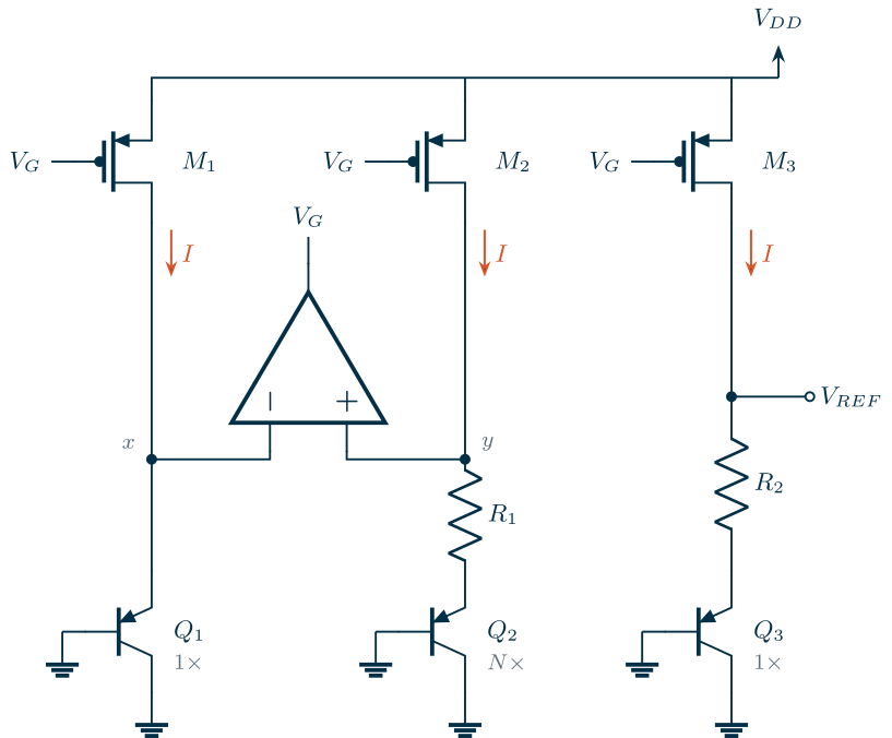
Figure 14.4 shows the classic CMOS bandgap core. Three equal PMOS current sources feed three branches. An error amplifier adjusts their common gate voltage until nodes \(x\) and \(y\) are equal. Then the voltage across \(R_1\) is the difference of two \(V_{EB}\) at the same current, \(Q_2\) having \(N\) times the area of \(Q_1\), and the branch current is PTAT. The third branch copies it through \(R_2\) into a third transistor:
Key equation · Voltage-mode bandgap
\[I = \frac{V_T\ln N}{R_1}, \qquad V_{REF} = V_{EB3} + \frac{R_2}{R_1}\,V_T\ln N, \qquad \frac{R_2}{R_1} = \frac{-\,\partial V_{EB}/\partial T\big\vert_{I\propto T}}{(k/q)\ln N}. \tag{14.4}\]The output depends on the ratio \(R_2/R_1\), not on either resistor, and on \(V_{EB}\) and \(V_T\), which the process cannot change much.
Worked example 14.1 · A bandgap in SKY130
Current and \(R_1\). Choose \(N\) = 8 and \(I\) = 2 µA at 27 °C: \(R_1 = V_T\ln 8/I\) = 53.8 mV / 2 µA = 26.9 kΩ.
Ratio. The branch current is PTAT, \(I \propto T\), which makes \(V_{EB}\) fall more slowly than at constant current: \(\partial V_T\ln I/\partial T\) adds \(k/q\) = 0.086 mV/K. So the slope to cancel is −1.85 + 0.09 = −1.77 mV/K, and \(R_2/R_1\) = 1.77/0.179 = 9.86, \(R_2\) = 265 kΩ.
Output. \(V_{REF}\) = 0.701 V + 9.86 × 53.8 mV = 1.232 V.
Devices. PMOS sources at \(g_m/I_D = 10\) and L = 2 µm (W = 10.6 µm from the tables) for a high output resistance;
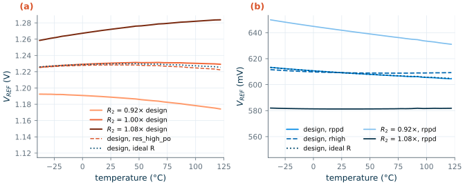
res_xhigh_po_0p35resistors, 2 kΩ/□, so \(R_2\) is about 46 µm long. The amplifier is modelled as an ideal 60 dB voltage amplifier, so we see the core alone.Simulation. \(V_{REF}\) = 1.2306 V at 27 °C, 1.3 mV below the hand value. Over −40 °C to 125 °C it stays within 5.9 mV, a temperature coefficient of 30 ppm/K by the box method (\(\Delta V/(V\cdot\Delta T)\)), with its maximum at 67 °C (Figure 14.5a).
Curvature and trimming
The bow in Figure 14.5a is curvature. Eq. (14.4) cancels the slope at one temperature only, because \(V_{EB}\) is not a straight line: Eq. (14.2) contains \(T\ln T\) terms from \(X_{TI}\). The residual is a parabola of a few millivolts, which limits a simple bandgap to roughly 10–30 ppm/K over the industrial range. Curvature-correction circuits add a small \(T\ln T\) term of the opposite sign; they are beyond this chapter [53].
In silicon, \(V_{EB}\) varies from wafer to wafer, so the slope cancels at a different temperature on every chip. Changing \(R_2\) by ±8 % tilts the curve and moves its peak to an end of the range (Figure 14.5a); the box TC rises to 96 and 124 ppm/K. Production bandgaps therefore include a trim: \(R_2\) is a chain of segments with switches or fuses, adjusted after a measurement at one temperature.
Try the trim yourself in the demo below: set \(R_2/R_1\) and watch the falling \(V_{EB}\), the rising \(K\cdot\Delta V_{EB}\) and their sum, simulated with the chapter’s netlists; the SG13G2 button switches to the current-mode core of Section 14.5.
The effect of real resistors
Because Eq. (14.4) contains only the ratio \(R_2/R_1\), the resistors’ large TC almost cancels. With res_high_po (+506 ppm/K) instead of res_xhigh_po (−1474 ppm/K), \(V_{REF}\) at 27 °C moves by 2.3 mV and the TC is 31 ppm/K; with ideal resistors it is 23 ppm/K. What does change is the current: with res_xhigh_po it rises by 119 % from −40 °C to 125 °C instead of the PTAT 71 %, so \(V_{EB}\) sees a different current and the curvature changes slightly. Two rules follow: build \(R_1\) and \(R_2\) from the same resistor type, with the same width and unit segments, so that their ratio survives process variation and temperature, and lay them out interleaved (Chapter 15).
Common pitfall · Forgetting the amplifier’s offset
The error amplifier’s input offset \(V_{OS}\) adds directly to \(\Delta V_{EB}\) across \(R_1\), and \(R_2/R_1\) multiplies it: \(\Delta V_{REF} \approx (R_2/R_1)V_{OS}\). With \(R_2/R_1\) = 9.9, the 3–5 mV rms offset of the OTA in Chapter 13 would become 30–50 mV rms, far more than all the curvature. Real bandgaps use large input devices, a larger \(N\) (which raises \(\Delta V_{EB}\) and lowers \(R_2/R_1\)), chopping, or trimming. The amplifier also needs an input range that includes \(V_{EB}\) from 0.51 V (125 °C) to 0.82 V (−40 °C).
Why not in SG13G2?
The output of Figure 14.4 is about 1.23 V, and the PMOS source above it needs a few hundred millivolts to stay in saturation. That fits under SKY130’s 1.8 V, but not under SG13G2’s 1.2 V core supply. One could move the circuit to SG13G2’s 3.3 V I/O devices; the next section shows how to stay at 1.2 V instead.
14.5 Low-voltage references
Banba and co-authors found a way to get a temperature-independent output below 1 V [80]: add currents instead of voltages. In Figure 14.6 each bipolar branch has a resistor \(R_2\) in parallel. With \(x = y\) forced by the amplifier, the current in each \(R_2\) is \(V_{EB}/R_2\), a CTAT current, and the current in \(R_1\) is \(V_T\ln N/R_1\), a PTAT current. Each PMOS carries their sum, and \(M_3\) copies it into \(R_3\):
Key equation · Current-mode (Banba) bandgap
\[I = \frac{V_{EB1}}{R_2} + \frac{V_T\ln N}{R_1}, \qquad V_{REF} = R_3 I = \frac{R_3}{R_2}\left(V_{EB1} + \frac{R_2}{R_1}V_T\ln N\right). \tag{14.5}\]The bracket is the same bandgap sum as Eq. (14.4), about 1.2 V; the ratio \(R_3/R_2\) scales it to any value, and the supply only needs to exceed \(V_{EB}\) plus the PMOS headroom.
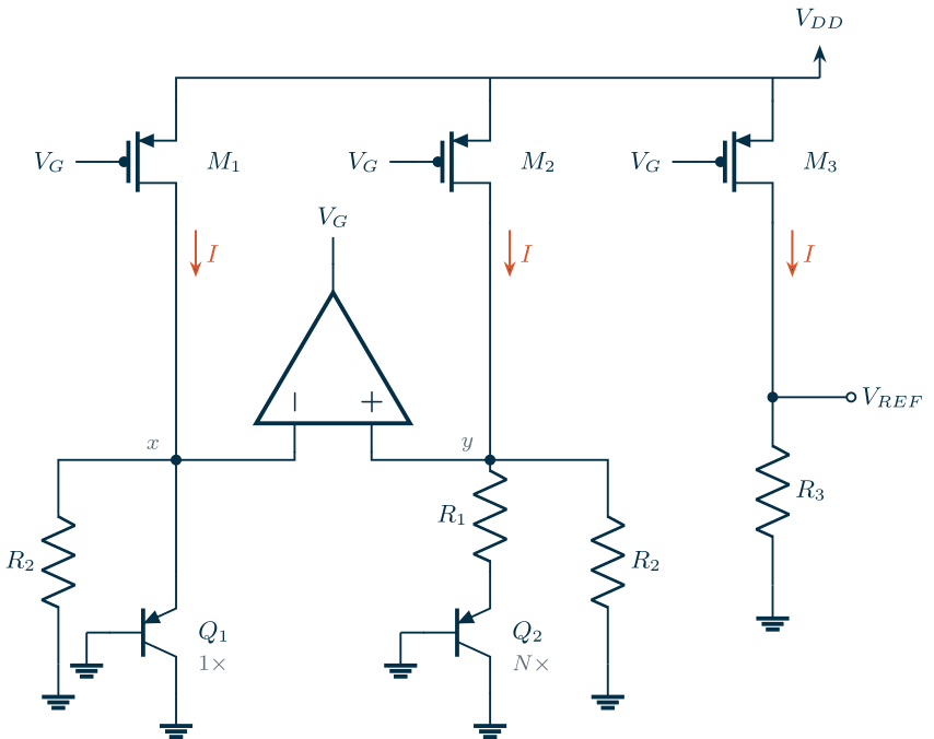
We designed it for SG13G2 at 1.2 V with the same recipe: \(N\) = 8, a PTAT current of 2 µA (\(R_1\) = 26.9 kΩ), \(R_2/R_1\) = 8.04 from the pnpMPA’s slope (−1.53 + 0.09 mV/K over 0.179 mV/K), so \(R_2\) = 216 kΩ, and \(R_3\) = 108 kΩ for an output of 0.6 V. Each branch carries 5.55 µA. Figure 14.5b shows the result with rppd resistors: 609.1 mV at 27 °C, but falling steadily with temperature, by 8.8 mV from −40 °C to 125 °C (90 ppm/K); with ideal resistors it is almost the same (87 ppm/K). The hand ratio leaves a residual slope here: it was set from the slope of \(V_{EB}\) at a single temperature, and second-order effects that Eq. (14.5) ignores, such as the curvature of \(V_{EB}\) and the different drain voltage of \(M_3\), shift the best ratio by a few percent. The \(R_2\) trims show how much: +8 % (\(R_2/R_1\) = 8.7) brings the TC down to 8 ppm/K (and the output to 581 mV, which a smaller \(R_3\) would restore), while −8 % raises it to 184 ppm/K.
The resistor type matters here too. With rhigh (−2300 ppm/K) the TC is 28 ppm/K, better than with rppd: Eq. (14.5) contains only ratios, but the branch currents now follow the resistors, and with rhigh they grow by about 49 % over the range, which happens to offset the residual slope. That is luck, not design: the resistor’s TC varies from lot to lot, and a trim is still needed.
The SG13G2 core stays within 2 mV of its nominal output down to a supply of 1.11 V, the SKY130 core down to 1.70 V; below that the PMOS sources leave saturation and the loop loses control (in SG13G2, ngspice even finds the zero-current state at 0.96 V, a reminder of Section 14.6). From the nominal supply up to +10 %, the output changes by −4.9 mV/V in SG13G2 and 15.5 mV/V in SKY130. This line regulation comes from the finite output resistance of the PMOS sources, whose drain voltages differ between branches; cascoding them, or regulating their supply, improves it by an order of magnitude.
Other topologies
The Brokaw cell [79] is the classic bipolar bandgap: two npn transistors with emitter areas in the ratio \(N\), a resistor in the emitter of the larger one, and an amplifier that forces equal collector currents. Its output is taken from the bases, and it needs no separate output branch. It suits processes with good npn transistors, such as SG13G2’s SiGe HBTs. Below 1 V, sub-bandgap references divide the bandgap sum with resistors, as Banba’s circuit does, or combine MOSFET threshold voltages in weak inversion with PTAT voltages; they trade accuracy for supply voltage and power.
What this means for your design
A bandgap is a ratio circuit. Its accuracy comes from matched bipolar transistors, matched resistors and a low-offset amplifier, not from any absolute value. Spend area on the amplifier’s input pair and on interleaved resistor and bipolar arrays, plan a trim, and simulate across temperature and Monte Carlo (Section 13.8). Expect 10–30 ppm/K untrimmed curvature and several millivolts of spread before trimming.
14.6 Start-up
Every self-biased circuit in this chapter has a second, unwanted operating point: all currents zero. In the beta-multiplier of Figure 14.1, if no current flows, \(M_1\) has no gate voltage, \(M_2\) is off, the PMOS gates float up to \(V_{DD}\) and nothing forces a current to start. Eq. (14.1) is satisfied by \(I = 0\) as well. Whether the circuit leaves this state at power-up depends on leakage and on how fast the supply rises, which is to say on luck.
Figure 14.2b shows it. The supply ramps from 0 to \(V_{DD}\) in 10 µs. Without a start-up circuit the SKY130 beta-multiplier is still at 1.64 pA after 60 µs, while the SG13G2 one does start, at 10.00 µA, because its thin-oxide transistors leak enough to kick it. A design that works only because of leakage in one corner will fail in another.
The start-up circuit in Figure 14.1 detects the zero state and injects current. A weak, always-on PMOS \(M_{S2}\) (W/L = 0.5/20 µm) pulls node \(s\) high; \(M_{S1}\) then pulls the PMOS gates down, which turns on the mirror. Once current flows, \(M_{S3}\), which mirrors \(M_1\), pulls \(s\) low and \(M_{S1}\) turns off, so the start-up circuit takes no part in normal operation. With it, both references reach 10.0 µA within 10 µs of the start of the ramp. Three rules make a start-up circuit safe:
- It must turn fully off in normal operation, or it adds an error current (check its current at the hottest, fastest corner).
- It must work over the whole supply ramp, slow and fast; simulate ramps of 1 µs and 1 ms.
- The bandgap has the same problem: with zero current, \(x = y = 0\), the error amplifier’s inputs are at ground and an NMOS input pair is off. A start-up circuit like Figure 14.1’s, sensing the PMOS gate or the branch current, is part of every bandgap.
Try it · Lab 4
Lab 4 builds the beta-multiplier that biases the course OTA. Add the start-up circuit of Figure 14.1, then run a transient with a supply ramp, with and without it, at the ss and ff corners and at −40 °C and 125 °C.
14.7 The low-dropout regulator
A regulator turns a noisy, varying supply into a clean, fixed one. The low-dropout regulator (LDO) does it with a single PMOS pass device between input and output, in a feedback loop that compares a divided copy of the output with a reference (Figure 14.7). The PMOS can work with its source-drain voltage down to a few hundred millivolts, hence low dropout [52]. In regulation
\[V_{OUT} = V_{REF}\left(1 + \frac{R_a}{R_b}\right). \tag{14.6}\]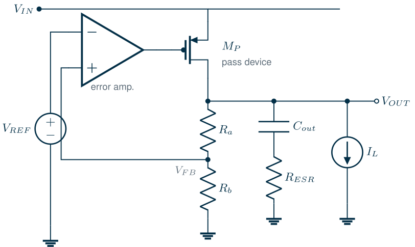
Design in both PDKs
Table 14.3 lists the two designs.
Table 14.3. The LDO in both PDKs (tt, 27 °C).
| Quantity | SG13G2 | SKY130 |
|---|---|---|
| \(V_{IN}\) → \(V_{OUT}\) | 1.2 V → 1.0 V | 1.8 V → 1.5 V |
| \(V_{REF}\) (from Section 14.5 / 14.4) | 0.6 V | 1.2 V |
| \(R_a\) / \(R_b\) (PDK resistors) | 80 / 120 kΩ, rhigh | 40 / 160 kΩ, res_xhigh_po |
| Pass device \(M_P\), at 5 mA, \(g_m/I_D\) = 8 | W/L = 600/0.18 µm | W/L = 650/0.18 µm |
| Error amplifier | 5T OTA, 5 µA per side | 5T OTA, 5 µA per side |
| Output capacitor | 1 µF, 0.1 Ω ESR (off chip) | 1 µF, 0.1 Ω ESR (off chip) |
The pass device is sized with the gm/ID tables for the full load of 5 mA at a source-drain voltage equal to the dropout, 0.2 V and 0.3 V. That makes it wide, 600 µm or more, so its gate capacitance is about 1 pF. The error amplifier is a small 5T OTA with an NMOS input pair at \(g_m/I_D\) = 20. The divider uses the high-resistivity poly of each PDK, 200 kΩ in total, so it draws 5 to 7.5 µA.
Loop stability
The loop has two poles. One is at the output: the load and divider resistance in parallel with the output resistance of \(M_P\), \(R_{out}\), against \(C_{out}\). The other is at the gate of \(M_P\): the output resistance of the error amplifier, \(R_{EA}\), against the gate capacitance. With a large external capacitor the output pole is dominant, and the loop crosses unity at about
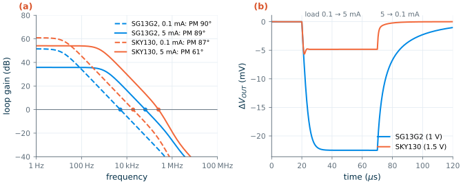
\[f_u \approx \frac{A_{EA}\,\beta\,g_{mP}}{2\pi C_{out}}, \qquad \beta = \frac{R_b}{R_a + R_b}, \qquad\text{stable if}\quad f_u \ll \frac{1}{2\pi R_{EA}C_{gate}}. \tag{14.7}\]Because \(g_{mP}\) grows with the load current, so does \(f_u\): an LDO is least stable at full load. We measure the loop gain by opening the loop at the feedback node for AC only, with a 1 GH inductor and a 1 F capacitor, the same trick as for the OTA in Chapter 13. Figure 14.8a shows it at 0.1 mA and 5 mA. In SG13G2 the loop gain at DC is 51.5 dB at light load and 35.8 dB at full load, with unity-gain frequencies of 5.13 kHz and 65.2 kHz and phase margins of 90° and 89°. In SKY130 the DC gains are 60.9 and 54.1 dB, \(f_u\) = 18.9 kHz and 249 kHz, and the phase margin falls from 87° to 61° at full load, as Eq. (14.7) predicts: the SKY130 error amplifier, with its higher intrinsic gain, puts the gate pole lower and the unity-gain frequency higher.
Load and line regulation
When the load current jumps, the output capacitor supplies the difference until the loop responds, about \(1/(2\pi f_u)\) later. In Figure 14.8b the SKY130 output dips by 5.7 mV after the step to 5 mA and settles within a few microseconds, a little higher, at its new DC value. The SG13G2 output falls by 22.5 mV and stays there: almost all of that is the DC load regulation, not a transient. When the load is removed, both outputs return with the time constant of the light-load loop, whose crossover is much lower (5.13 kHz in SG13G2, so about 30 µs). In DC, the loop gain divides the output resistance of the pass device: the load regulation is 4.16 mV/mA in SG13G2 and 0.87 mV/mA in SKY130, and the line regulation at full load 17.4 and −15.0 mV/V. SG13G2 is about five times worse on load regulation because its loop gain at full load is 18 dB lower: the 1.2 V devices have less intrinsic gain, both in the error amplifier and in the pass device. A two-stage error amplifier (Chapter 12) would fix this, at the cost of a third pole to compensate. The dropout at 5 mA, the input voltage at which the output falls 10 mV below its target, is 0.16 V in SG13G2 and 0.08 V in SKY130.
SG13G2 vs SKY130 · Regulators for a 1.2 V core
Our SG13G2 LDO runs from the 1.2 V core supply to show the principle with core devices. A real SG13G2 chip would more likely regulate a 3.3 V input down to 1.2 V, with the thick-oxide
sg13_hv_pmosas the pass device and the error amplifier on the 3.3 V supply, which also gives it more gain. In SKY130 the same role is played by the 5 V devices (pfet_g5v0d10v5). Fully on-chip LDOs without a microfarad capacitor exist, but they need a compensated multi-stage loop that is beyond an introduction.
- A beta-multiplier makes a supply-independent current, but it drifts by tens of percent over temperature and has a zero-current state that needs a start-up circuit.
- \(V_{BE}\) falls by 1.5–1.9 mV/K (CTAT); the difference of two \(V_{BE}\) at area ratio \(N\) rises by \((k/q)\ln N\) (PTAT). Their weighted sum is the bandgap voltage, about 1.2 V. Eq. (14.3) predicted the PDK slopes within 2 %.
- The voltage-mode core gives 1.23 V in SKY130 with a TC of about 30 ppm/K; the current-mode (Banba) core gives 0.6 V from SG13G2’s 1.2 V supply with 90 ppm/K as designed by hand and 8 ppm/K after an 8 % trim of \(R_2\). What remains is curvature; process spread needs a trim.
- Bandgaps depend on ratios: use one resistor type for all resistors, matched bipolar arrays, and an amplifier with low offset, which \(R_2/R_1\) amplifies about tenfold.
- An LDO is a feedback amplifier whose second pole moves with the load current; check stability at full load. Loop gain sets load and line regulation, and SG13G2’s lower intrinsic gain shows up directly.
Further reading
- B. Razavi, Design of Analog CMOS Integrated Circuits [51], chapter 12: bandgap references, PTAT currents and start-up, with clear derivations.
- H. Banba et al. [80]: the original current-mode bandgap paper, short and readable.
- A. P. Brokaw [79]: the classic three-terminal bandgap cell.
- P. R. Gray, P. J. Hurst, S. H. Lewis and R. G. Meyer [53]: the bipolar background of references, including curvature.
- T. Chan Carusone, D. A. Johns and K. W. Martin [52]: references and voltage regulators in one chapter.