Chapter 8
Current Mirrors and Biasing
Analog circuits run on currents copied from a single reference. A good mirror copies accurately over a wide voltage range, and a good reference does not care about the supply. Both are harder at 1.2 V than at 1.8 V.
- Design a basic current mirror with gm/ID, estimate its copying error from the lookup tables, and choose its length.
- Build accurate mirror ratios from unit devices, and explain why scaled widths and lengths fail.
- Raise output resistance with cascode and wide-swing cascode mirrors, and work out the headroom each needs at 1.2 V and 1.8 V.
- Design a constant-gm (beta-multiplier) current reference with a start-up circuit, and check it across supply and temperature.
- Plan how a 10 µA reference current is distributed to the blocks of a chip.
Contents
In Chapter 7 every bias came from an ideal current source or an ideal voltage source. On a chip there is exactly one accurate current, the reference, and every other bias current is a copy of it, made by a current mirror. The course project (Section 1.6) receives a single 10 µA reference and must derive the currents of both OTA stages from it. This chapter builds the pieces: the mirror, its errors, its improved forms, a reference that generates the 10 µA in the first place, and the plan that distributes it. All simulations are in tools/figs/ch08_mirrors.py (tt, 27 °C unless stated).
8.1 The basic mirror
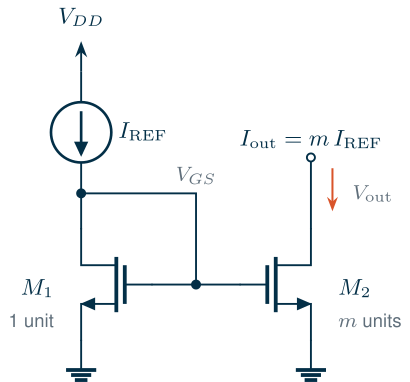
A diode-connected transistor \(M_1\) (Figure 8.1) converts the reference current into a gate–source voltage: it settles at exactly the \(V_{GS}\) at which it carries \(I_\mathrm{REF}\). A second transistor \(M_2\) with the same \(V_{GS}\) then carries the same current, or a scaled one. If both are in saturation and have the same length,
\[I_\mathrm{out} = \frac{(W/L)_2}{(W/L)_1}\, I_\mathrm{REF} = m\, I_\mathrm{REF}, \tag{8.1}\]where in a good layout the ratio \(m\) is a number of identical unit devices: \(M_1\) is one unit and \(M_2\) is \(m\) units in parallel. Nothing in Eq. (8.1) depends on the threshold voltage or the mobility. This is why mirrors work so well: the process parameters cancel between two neighbouring transistors.
Sizing a mirror with gm/ID
The design choices are the inversion level and the length. Section 6.2 placed current sources in strong inversion, at \(g_m/I_D\) of 5 to 10 V⁻¹: a large overdrive makes the current less sensitive to threshold mismatch (Chapter 13) and gives a small device. We use \(g_m/I_D = 8\ \mathrm{V^{-1}}\) throughout. The price is headroom: the output transistor needs a drain–source voltage of at least
\[V_{DS,\mathrm{sat}} \approx \frac{2}{g_m/I_D}, \tag{8.2}\]about 0.25 V at 8 V⁻¹, to stay in saturation (Eq. (7.12)). The length sets the accuracy, as the next section shows. At 10 µA and L = 1 µm the tables give W = 1.08 µm and \(V_{GS}\) = 0.47 V in SG13G2, and W = 1.41 µm and 0.82 V in SKY130.
Ratios from unit devices
Eq. (8.1) suggests three ways to make a 1:4 mirror: four times the width, a quarter of the length, or four copies of the same device. Only the third is reliable. Table 8.1 compares them for a 10 µA to 40 µA mirror at L = 1 µm, with both drains at the same voltage so that only the geometry differs.
Table 8.1. Error of a 1:4 NMOS mirror (10 µA in, L = 1 µm, equal drain voltages) for different ways of making the ratio.
| How \(M_2\) is made (\(M_1\) = one 5 µm finger unless stated) | SG13G2 | SKY130 |
|---|---|---|
| four unit devices (\(m = 4\)) | 0.0 % | 0.0 % |
one 20 µm device in 5 µm fingers (ng=4 / nf=4) |
0.0 % | 0.0 % |
| one 20 µm device in as few fingers as allowed (2 × 10 µm / 1 × 20 µm) | +25.4 % | +32.5 % |
| ratio by width with narrow devices (1 µm → 4 µm) | +13.4 % | +12.0 % |
| ratio by length (5/4 µm → 5/1 µm) | −30.5 % | −29.0 % |
The unit-device mirror is exact in both PDKs, and so is a device split into fingers of the unit width. Everything else fails by 12 to 33 %. A ratio by length fails because the effective channel length differs from the drawn one by a fixed amount and because short-channel effects change the threshold voltage with L (Section 4.6). A ratio by width fails at narrow widths for a similar reason (the edges of the channel matter more), and in SKY130 also at large finger widths, because the model is split into separately fitted bins of W and L, as Section 6.6 warned. Even SG13G2, whose model has no bins, changes by 25 % between 5 µm and 10 µm fingers at this low current density, where a few millivolts of threshold shift matter.
Common pitfall · Making a ratio with W or L
Never set a mirror ratio by scaling a single transistor’s width or length. Choose a unit device (in SKY130, one finger of about 5 µm, the width of the lookup tables) and build every device of the mirror from it, with the multiplier
mor with fingers of the same width. Non-integer ratios such as 2:3 are made from integer numbers of units on both sides. The same unit devices are also what make a common-centroid layout possible (Chapter 15).
8.2 Mirror errors
A mirror’s copy can be wrong for three reasons:
- Systematic error. The two transistors see different drain voltages, and channel-length modulation and DIBL make the current depend on \(V_{DS}\).
- Random error. Neighbouring transistors are never identical; their thresholds and current factors differ randomly. This mismatch scales with \(1/\sqrt{WL}\) and is the subject of Section 13.6.
- Layout and environment errors: ground-voltage differences, temperature gradients and stress, which Section 8.6 and Chapter 15 deal with.
This section treats the first. \(M_1\) always works at \(V_{DS} = V_{GS}\); \(M_2\) works at whatever voltage its load imposes. With the Early voltage \(V_A = I_D/g_{ds}\) of Eq. (7.2),
Key equation · Systematic error of the basic mirror
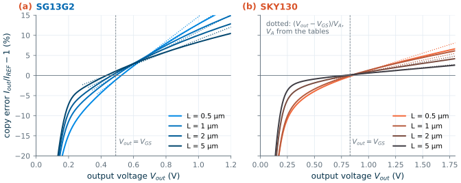
\[\frac{I_\mathrm{out}}{m\,I_\mathrm{REF}} - 1 \approx \frac{V_\mathrm{out} - V_{GS}}{V_A}, \qquad R_\mathrm{out} = r_{o2} = \frac{V_A}{I_\mathrm{out}}. \tag{8.3}\]The copy is exact only when the output sits at \(V_{GS}\). The lookup tables give \(V_A = (g_m/g_{ds})/(g_m/I_D)\) for every length.
Figure 8.2 plots the error against the output voltage for four lengths, each sized for 10 µA at 8 V⁻¹. The dotted lines are Eq. (8.3) with \(V_A\) from the tables; they follow the simulation to within a few tenths of a percent wherever the output transistor is saturated.
Three things stand out.
- SKY130 is about six times more accurate. At \(V_\mathrm{out} = V_{DD}/2\) the error is 0.35–0.56 % in SKY130 and 2.4–3.0 % in SG13G2. With the output at the supply it reaches 2.6–6.6 % and 10–17 %. The cause is the Early voltage: 18 V for a 1 µm SKY130 device at this bias, 4.0 V for SG13G2, the same thin-oxide, short-channel behaviour that gave SG13G2 its low intrinsic gain in Chapter 6.
- Length helps less than you might expect. Going from 0.5 to 5 µm doubles \(V_A\) in SG13G2 (3.2 to 6.4 V), but it also lowers \(V_{GS}\) (0.52 to 0.43 V), so the voltage difference at mid-supply grows and the error there hardly changes. Length pays off over a range of output voltages: at the supply the error falls from 17 % to 10 %.
- Below about 0.2 V the current collapses, as \(M_2\) leaves saturation. Eq. (8.2) gives 0.25 V for the edge; the curves bend over between 0.15 and 0.3 V.
What this means for your design
Choose L for mirrors from the error you can tolerate over the output range the mirror will really see, using Eq. (8.3) with the table’s \(V_A\): 1–2 µm is a good start in SKY130, 2–5 µm in SG13G2. Where the output voltage of a mirror is set by the circuit (for example the two branches of a differential pair), design so that it sits near \(V_{GS}\). Where it swings, or where you need better than a few percent in SG13G2, use a cascode.
8.3 Cascode and wide-swing mirrors
A cascode transistor on top of \(M_2\) holds \(M_2\)’s drain still, exactly as in Section 7.6. The standard cascode mirror (Figure 8.3(a)) biases the cascode \(M_4\) with a second diode \(M_3\) stacked on \(M_1\). Because \(V_{GS3} \approx V_{GS4}\), node X sits at \(V_{GS1}\), so \(M_1\) and \(M_2\) have the same drain voltage and the systematic error of Eq. (8.3) disappears. The output resistance rises by about the intrinsic gain of \(M_4\):
\[R_\mathrm{out} \approx (1+\eta_4)\,\frac{g_{m4}}{g_{ds4}}\; r_{o2}. \tag{8.4}\]The cost is headroom. The output must stay above \(V_X + V_{DS,\mathrm{sat}}\):
\[V_\mathrm{out,min} = V_{GS} + V_{DS,\mathrm{sat}} \qquad \text{(standard cascode)}. \tag{8.5}\]That is \(0.47 + 0.25 = 0.72\) V in SG13G2 and \(0.82 + 0.25 = 1.07\) V in SKY130: more than half the supply in both. The output transistor of a basic mirror is wasting a whole threshold voltage of headroom, because node X sits at \(V_{GS}\) when \(V_{DS,\mathrm{sat}}\) would do.
The wide-swing (or low-voltage) cascode mirror [51, 53, 55] fixes this (Figure 8.3(b)). Its cascode gates are driven from a separate bias \(V_B\), chosen so that \(M_1\) and \(M_2\) sit just inside saturation:
\[V_B = V_{DS1} + V_{GS3}, \quad V_{DS1} = V_{DS,\mathrm{sat}} + \text{margin}, \qquad V_\mathrm{out,min} = V_{DS1} + V_{DS,\mathrm{sat}} \approx 2V_{DS,\mathrm{sat}} + \text{margin}. \tag{8.6}\]In the reference branch, the gate of \(M_1\) is taken from the top of the branch (the drain of \(M_3\)), so \(M_1\) still carries exactly \(I_\mathrm{REF}\) and \(M_2\), with the same \(V_{GS}\) and the same \(V_{DS}\), copies it. We choose \(V_{DS1}\) = 0.30 V (0.25 V plus 50 mV of margin) in both PDKs. \(V_B\) comes from a diode-connected \(M_5\), made narrower and longer than the unit so that it needs a larger \(V_{GS}\) at the same current: a short simulation gives the \(V_{GS3}\) the cascode needs at \(V_{SB}\) = 0.30 V (0.53 V and 0.89 V), and the tables then give \(M_5\)’s width at L = 4 µm.
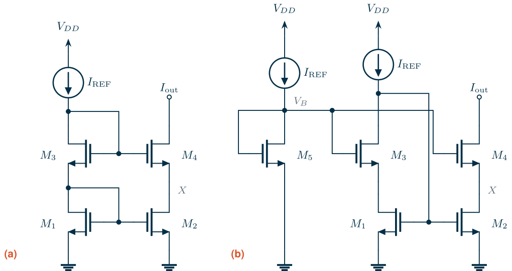
Figure 8.4 compares the three mirrors at 10 µA with L = 1 µm. Both cascodes are flat where the basic mirror slopes, and their output resistance is 20 to 80 times higher. The knees, the lowest output voltage at which \(R_\mathrm{out}\) is still within a factor of ten of its full value, are listed in Table 8.2 together with the hand estimates.
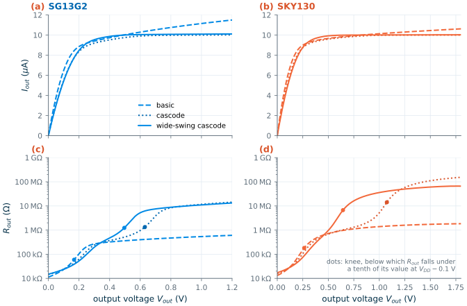
Table 8.2. Headroom of the three mirrors at 10 µA (L = 1 µm, gm/ID = 8 V−1): minimum output voltage by hand (Eqs. 8.2, 8.5, 8.6), simulated knee, and output resistance near the top of the range.
| Mirror | SG13G2 hand | SG13G2 knee | SG13G2 \(R_\mathrm{out}\) | SKY130 hand | SKY130 knee | SKY130 \(R_\mathrm{out}\) |
|---|---|---|---|---|---|---|
| basic | 0.25 V | 0.17 V | 574 kΩ | 0.25 V | 0.26 V | 1.8 MΩ |
| standard cascode | 0.72 V | 0.63 V | 13.0 MΩ | 1.07 V | 1.07 V | 141.5 MΩ |
| wide-swing cascode | 0.55 V | 0.50 V | 12.2 MΩ | 0.55 V | 0.64 V | 66.1 MΩ |
| Supply | 1.2 V | 1.8 V |
SG13G2 vs SKY130 · Headroom at 1.2 V and 1.8 V
The wide-swing cascode needs about the same voltage in both PDKs, because it costs two saturation voltages and those depend on \(g_m/I_D\), not on the process. The standard cascode costs a threshold voltage more, and here the PDKs differ: SKY130’s NMOS needs about 0.35 V more gate voltage at the same inversion level, so its standard cascode needs 1.07 V by hand. Its reference branch is worse still: two stacked diodes need 1.81 V at 10 µA, more than the 1.8 V supply leaves once a real current source sits above them (1.04 V in SG13G2). In SKY130 the standard cascode mirror barely fits; in SG13G2 its knee sits at more than half the supply. Use the wide-swing form in both. The price of the wide-swing mirror is the extra bias branch, which costs another \(I_\mathrm{REF}\) (shared by every mirror that uses the same \(V_B\)), and a bias voltage that must track the process: here \(M_5\), at 0.55 µm and 0.79 µm wide, is far narrower than the table width, and its \(V_{GS}\) came out 49 mV (SG13G2) and 86 mV (SKY130) above the table’s prediction. That is the safe direction (more margin for \(M_1\)), but check \(V_{DS1}\) at every corner.
Try it · Lab 4
Lab 4 builds the three mirrors of Figure 8.4 in your PDK, sweeps their outputs, and then runs a Monte Carlo analysis to compare the systematic error of this section with the random error of Chapter 13.
8.4 Supply-independent references
Where does \(I_\mathrm{REF}\) come from? A resistor from the supply would give a current that changes with \(V_{DD}\), with the threshold voltage and with temperature. The constant-gm reference, or beta multiplier, makes a current that depends on a resistor and on transistor ratios only [51, 55, 52]. It is shown in Figure 8.5.
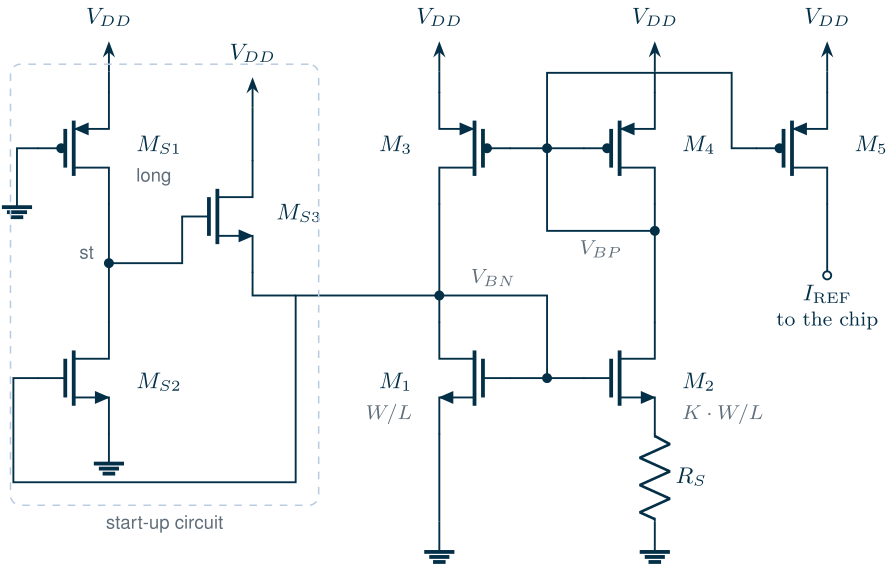
The PMOS mirror \(M_3\), \(M_4\) forces equal currents in the two branches. \(M_2\) is \(K\) times wider than \(M_1\), so at the same current it needs a smaller gate–source voltage, and the difference appears across \(R_S\):
Key equation · The beta-multiplier current
\[V_{GS1} = V_{GS2} + I_\mathrm{REF}R_S \quad\Longrightarrow\quad R_S = \frac{V_{GS1}(I_\mathrm{REF}) - V_{GS2}(I_\mathrm{REF}/K)}{I_\mathrm{REF}}, \tag{8.7}\]where \(V_{GS2}\) is read at \(1/K\) of \(M_1\)’s current density. In strong inversion (square law) this gives \(g_{m1} = \tfrac{2}{R_S}\left(1 - 1/\sqrt{K}\right)\); in weak inversion \(I_\mathrm{REF} = nU_T\ln K/R_S\) and \(g_{m1}R_S = \ln K\). In both limits \(g_{m1}\) is set by \(R_S\) alone, hence the name.
The supply voltage does not appear in Eq. (8.7): to first order the current is independent of \(V_{DD}\). Two second-order effects remain. Channel-length modulation lets the branch currents differ when \(V_{DD}\) changes the drain voltages of \(M_2\) and \(M_3\), and the current follows the resistor’s temperature coefficient and the mobility. With lookup tables we need neither the square law nor the weak-inversion formula: Eq. (8.7) is evaluated directly.
Worked example 8.1 · A 10 µA constant-gm reference
Choices. \(K = 4\); L = 2 µm for every transistor (for \(V_A\), Section 8.2); \(M_1\) at \(g_m/I_D = 12\ \mathrm{V^{-1}}\) (moderate inversion: a larger \(V_{GS}\) difference than weak inversion, less headroom than strong inversion); PMOS mirror at 8 V⁻¹.
Widths. At 10 µA the tables give \(W_1\) = 5.76 µm in SG13G2 and 6.12 µm in SKY130; \(M_2\) is four of these in parallel. The PMOS devices are 8.75 µm and 10.40 µm wide.
Resistor. The tables give \(V_{GS1}\) = 0.346 V and, at a quarter of the current density, \(V_{GS2}\) = 0.255 V in SG13G2 (0.714 V and 0.623 V in SKY130). Eq. (8.7) gives \(R_S\) = 9.14 kΩ and 9.14 kΩ, and predicts \(g_{m1}R_S = 12 \times 0.091 = 1.10\), between the strong-inversion value (1.0) and the weak-inversion value (ln 4 = 1.39).
Simulation, first pass. With these resistors the reference delivers 9.08 µA in SG13G2 and only 6.87 µA in SKY130. The tables assume \(V_{SB} = 0\), but \(M_2\)’s source sits at \(I_\mathrm{REF}R_S \approx\) 90 mV, and the body effect raises its threshold by several millivolts: a large fraction of a 91 mV difference, and larger in SKY130, whose body effect is stronger (Section 7.4).
Second pass. Simulating eleven copies with scaled resistors in one run and interpolating gives \(R_S\) = 8.48 kΩ (SG13G2) and 6.80 kΩ (SKY130) for 10.0 µA. The resistors are high-resistance poly: the SG13G2
rhigh(0.5 µm wide, 2.97 kΩ per µm of length) and the SKY130res_high_po_0p35(1.14 kΩ per µm) [17, 18].
Figure 8.6 shows the finished references. Panel (a) sweeps the supply (with the start-up circuit of Section 8.5). The current switches on once \(V_{DD}\) can hold \(V_{GS1}\) plus a PMOS \(V_{SG}\), at 0.98 V in SG13G2 and 1.41 V in SKY130, and then rises only slowly: between 0.9 and 1.1 \(V_{DD}\) the sensitivity is 41 %/V in SG13G2 and 14 %/V in SKY130. The SG13G2 reference is three times more sensitive for the same reason its mirrors are less accurate: its Early voltage is lower. Cascoding the PMOS and NMOS mirrors (Section 8.3) would reduce both numbers by roughly the intrinsic gain, at the cost of headroom.
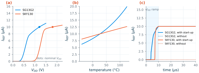
Panel (b) sweeps temperature from −40 °C to 125 °C. The SG13G2 current rises from 6.2 µA to 19.9 µA, the SKY130 current from 8.1 µA to 12.7 µA. The constant-gm property holds approximately: \(g_{m1}\) varies by 22 % in SG13G2 and 8 % in SKY130 over the range. The current varies much more: as the mobility falls with temperature, the transistors need more current for the same \(g_m\), and the resistor’s own temperature coefficient adds to that. The SG13G2 rhigh resistor has a large negative coefficient (−2235 ppm/K in our simulation), which makes its reference strongly temperature-dependent; the SKY130 resistor has +527 ppm/K. A current with a defined temperature behaviour needs a bandgap-based reference, the subject of Chapter 14. For biasing amplifiers, a constant-gm current is often exactly what is wanted, because it keeps the transconductances, and hence the bandwidths, of the circuits it biases nearly constant [52].
8.5 Start-up circuits
The beta multiplier has a second solution. If no current flows, \(M_1\) has no \(V_{GS}\), the PMOS mirror has nothing to copy, and the circuit is perfectly happy to stay off. Both states satisfy Kirchhoff’s laws. A start-up circuit removes the zero-current state: it detects that the circuit is off and injects a current until the loop takes over, and then it switches itself off.
The start-up of Figure 8.5 uses three small transistors. A long PMOS \(M_{S1}\), permanently on, pulls node st up through a weak current (0.84 µA in SG13G2, 0.64 µA in SKY130). As long as the reference is off, st is high and \(M_{S3}\) pushes current from \(V_{DD}\) into the diode \(M_1\), which starts the loop. Once \(V_{BN}\) rises, \(M_{S2}\) pulls st low and \(M_{S3}\) turns off. The start-up current through \(M_{S1}\) flows forever, so it is made long and narrow (0.5/20 µm here).
Figure 8.6(c) shows what happens without it. The supply ramps from zero in 10 µs, and every node starts at 0 V (ngspice’s uic option). Without a start-up circuit the SKY130 reference stays off for the whole 40 µs, at a few picoamperes. With it, the current reaches 90 % of its final value 7.9 µs after the ramp begins (8.2 µs in SG13G2), before the supply has settled. The SG13G2 reference without start-up circuit started anyway, pushed by the leakage currents of its thin-oxide transistors; that is luck, not design, because leakage depends strongly on corner and temperature. Note also what the DC analyses did: the operating point and the supply sweep of panel (a) found the running state with or without the start-up circuit, in both PDKs, even when we gave ngspice the zero state as its initial guess. A DC simulation simply does not tell you whether a circuit starts.
Common pitfall · Trusting a simulation that starts by itself
A DC operating point normally finds the “good” solution of a self-biased circuit, because the simulator’s initial guess happens to be near it. That proves nothing about the chip. Always check the start-up explicitly: ramp the supply in a transient with
uicfrom all-zero initial conditions, at every corner and at the temperature extremes, and also check that the start-up circuit turns off and does not disturb the reference once it is running (Chapter 14 does the same for the bandgap).
8.6 Distributing bias
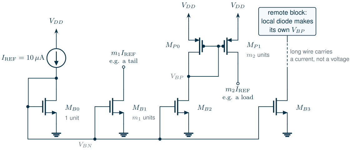
A chip has one reference and many blocks. Figure 8.7 shows how its current reaches them, and the rules behind it.
-
Send currents, not voltages. A bias voltage sent across a chip picks up every millivolt of ground drop between its source and its destination, and a mirror converts that error into current with a gain of \(g_m/I_D\):
\[\frac{\Delta I}{I} = \frac{g_m}{I_D}\,\Delta V. \tag{8.8}\]At 8 V⁻¹, a 5 mV difference between two grounds is a 4 % current error. A bias current sent over the same wire arrives intact, and a local diode turns it back into a voltage referred to the local ground.
- Use one unit device per bias type. Every NMOS mirror device in the chip is a multiple of the same NMOS unit and every PMOS device a multiple of the same PMOS unit. Ratios are then exact (Table 8.1), and the layout can interleave them.
- Mirror in strong inversion with a long channel, at 5–10 V⁻¹ and 1–5 µm (Section 8.2), and cascode where the accuracy or the supply rejection must be better.
- Decouple the bias lines. A high-impedance gate line running past switching signals picks up their edges. A small capacitor from \(V_{BN}\) to ground and from \(V_{BP}\) to \(V_{DD}\) keeps it quiet.
The course project follows exactly this plan (Chapter 12). The 10 µA reference, from an external source or from a reference like that of Worked example 8.1, enters the OTA’s diode-connected NMOS \(M_8\), one unit. The tail source \(M_5\) is two units (20 µA) and the second-stage current source \(M_7\) six units (60 µA), all NMOS sinks on the same \(V_{BN}\), as \(M_{B0}\) and \(M_{B1}\) in Figure 8.7. The unit follows the rules of this chapter: in SKY130 a 5 µm finger at L = 2 µm, in SG13G2 a 2.82 µm finger at L = 5 µm, the longer length buying back some of SG13G2’s lower Early voltage. Chapter 12 keeps these mirrors basic, because the second stage’s output must swing from 0.2 V to \(V_{DD} - 0.2\) V, which leaves room for a single device only; the systematic error this costs is the one of Figure 8.2.
What this means for your design
A bias network is a small circuit with a large influence. Its systematic errors set the currents of every block, its output resistance sets how much the supply leaks into them, and its start-up decides whether the chip works at all. In SG13G2 the low Early voltage makes all three harder: plan longer devices, cascodes where accuracy matters, and generous margins in Table 8.2’s terms. Random mismatch, the other half of the accuracy budget, is quantified in Section 13.6.
- A mirror copies a current through a shared \(V_{GS}\). Make ratios from identical unit devices: scaled widths or lengths were 12–33 % off in our simulations.
- The basic mirror’s systematic error is \((V_\mathrm{out}-V_{GS})/V_A\), with \(V_A\) straight from the lookup tables: about 3 % at mid-supply in SG13G2 and 0.5 % in SKY130.
- Cascodes remove that error and raise \(R_\mathrm{out}\) by the intrinsic gain. The standard cascode costs \(V_{GS} + V_{DS,\mathrm{sat}}\) of headroom; the wide-swing cascode only about \(2V_{DS,\mathrm{sat}}\), which is the only practical choice at 1.2 V and the better one at 1.8 V.
- A beta multiplier gives a supply-independent current set by a resistor; design it with Eq. (8.7) and the tables, then trim the resistor in simulation for the body effect of \(M_2\).
- Every self-biased reference needs a start-up circuit, verified by a supply-ramp transient from zero.
- Distribute currents, not voltages, and convert them to voltages locally.
Further reading
- B. Razavi, Design of Analog CMOS Integrated Circuits, Chapters 5 and 12 [51]: current mirrors, cascode mirrors and supply-independent biasing.
- R. J. Baker, CMOS: Circuit Design, Layout, and Simulation [55]: the beta-multiplier reference and its start-up circuits, with many practical variants.
- P. R. Gray et al. [53]: the most thorough analysis of mirror errors and of the wide-swing cascode.
- T. Chan Carusone, D. A. Johns and K. W. Martin [52]: constant-transconductance biasing and why it suits amplifiers.
- A. Hastings, The Art of Analog Layout [60]: unit devices and matched layout for mirrors.