Chapter 20
Comparators
A comparator turns the sign of a small voltage into a logic level. An amplifier does it slowly; a latch does it in a fraction of a nanosecond, because its positive feedback makes the difference grow exponentially. This chapter builds the StrongARM latch, the most common comparator of data converters, in both PDKs, and measures its speed, energy, offset and kickback.
- Explain why a latch decides faster than an amplifier, and derive the delay of a regenerative comparator.
- Describe the three phases of the StrongARM latch: reset, integration and regeneration.
- Extract the regeneration time constant from a simulation and use it to predict delay and metastability.
- Estimate the offset of a comparator from Pelgrom’s law, and measure it by Monte Carlo simulation.
- Estimate the noise of a dynamic comparator, and recognise kickback and how to reduce it.
Contents
20.1 What a comparator does
A comparator compares two voltages and gives a logic output: 1 if \(V_{in+} > V_{in-}\), 0 otherwise. Every analog-to-digital converter of Chapter 21 is built around them: a flash converter of N bits uses \(2^N - 1\) comparators in parallel, a successive-approximation converter one comparator N times per sample. The comparators of converters are clocked: they decide once per clock period, at an instant set by the clock, and are reset in between.
Four numbers describe a comparator. Its delay is the time from the clock edge to a valid logic output, and it grows as the input gets smaller. Its offset is the input at which it changes its decision, which mismatch moves away from zero (Chapter 13). Its noise makes the decision random for inputs close to the offset. And its energy per decision sets the power of a converter that makes billions of them per second. Two more matter in a system: metastability, a decision that has not finished when it is needed, and kickback, the disturbance the comparator couples back onto its inputs.
20.2 Amplification and regeneration
An open-loop amplifier can serve as a comparator: its output saturates at one rail or the other. But for a small input it is slow. An OTA with unity-gain frequency \(f_u\) behaves, above its dominant pole, like an integrator, and its output moves at \(2\pi f_uV_{in}\) volts per second. To swing by \(V_{sw}\), about half the supply, it needs
\[t_d \approx \frac{V_{sw}}{2\pi f_u\,V_{in}}, \tag{20.1}\]a delay inversely proportional to the input. The course OTA of Chapter 12 (\(f_u\) = 21.5 MHz) would need 4.4 µs to resolve 1 mV by this estimate; simulated open loop, it needs even longer, 12.6 µs in SG13G2 and 27 µs in SKY130, because its output must first leave the rail it sat on.
A latch uses positive feedback instead. Two cross-coupled inverters, each with transconductance \(g_m\) and load capacitance \(C\), form a loop with a gain greater than one; a voltage difference \(\Delta V\) between their outputs drives a current \(g_m\Delta V\) that makes the difference larger, \(C\,d\Delta V/dt = g_m\Delta V\):
Key equation · Regeneration
\[\Delta V(t) = \Delta V_0\,e^{t/\tau}, \qquad \tau = \frac{C}{g_m}. \tag{20.2}\]The difference grows exponentially with the regeneration time constant \(\tau\), and the time to reach a swing \(V_{sw}\) grows only with the logarithm of the initial difference: \(t = \tau\ln(V_{sw}/\Delta V_0)\).
Every factor of ten less input costs the same extra time, \(\tau\ln 10 \approx 2.3\tau\). With \(\tau\) of the order of 50 ps in our processes, a latch resolves a microvolt in less than a nanosecond, where by Eq. (20.1) the amplifier would need several milliseconds. The latch has two weaknesses: it must start from a balanced state, so it needs a reset, and a mismatch between its two halves is a large offset, since nothing amplifies the input before the feedback takes over. Practical comparators therefore put a stage of gain in front of the latch: a preamplifier [102], or, in the StrongARM latch, a differential pair that works only during the decision.
20.3 The StrongARM latch
The StrongARM latch of Figure 20.1 [103, 107] combines a differential pair \(M_1\)–\(M_2\), a cross-coupled pair of inverters \(M_3\)–\(M_6\) and four reset switches \(M_7\)–\(M_{10}\), with a clocked tail \(M_0\). It draws current only while it decides, and its outputs are full logic levels. A decision has three phases:
- Reset (CLK low). \(M_0\) is off, and \(M_7\)–\(M_{10}\) charge the nodes P, Q, X and Y to \(V_{DD}\).
- Integration (CLK rises). \(M_0\) turns on and the input pair discharges P and Q, the side with the larger input faster. Until P and Q have fallen far enough for \(M_3\) and \(M_4\) to conduct, the input difference is integrated onto their capacitance as a growing voltage difference.
- Regeneration. \(M_3\) and \(M_4\) conduct, X and Y follow P and Q down, and once they have fallen by a PMOS threshold the cross-coupled inverters regenerate: one output returns to \(V_{DD}\) and the other falls to ground.
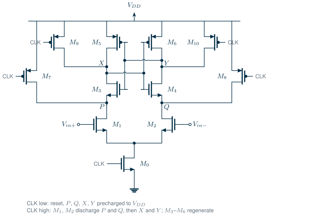
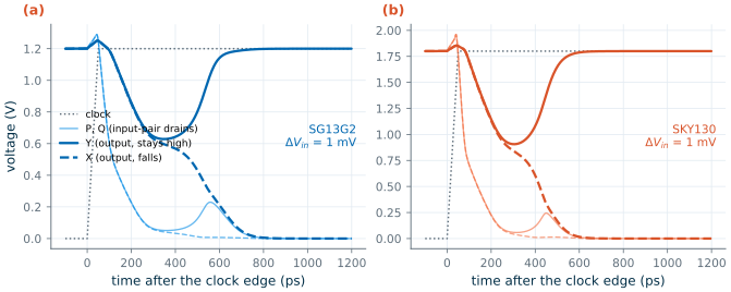
Figure 20.2 shows one decision of a 1 mV input in both PDKs. P and Q fall within about 200 ps; X and Y follow them down together, because the 1 mV difference is still small; then they separate, Y returns to \(V_{DD}\) and X falls to ground. With the same transistor widths in both PDKs, the decision takes 0.51 ns in SG13G2 and 0.41 ns in SKY130, whose larger supply gives every transistor more overdrive.
20.4 Delay and the regeneration time constant
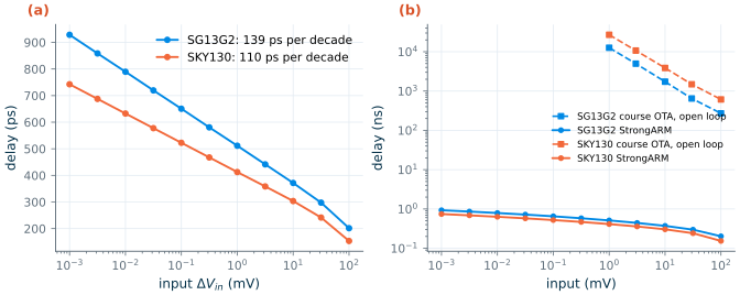
Figure 20.3a plots the delay, from the clock edge to an output difference of \(V_{DD}/2\), for inputs from 1 µV to 100 mV. Below about 10 mV it is a straight line against the logarithm of the input, as Eq. (20.2) predicts:
\[t_d = t_0 + \tau\ln\frac{V_{sw}}{G\,\Delta V_{in}}, \tag{20.3}\]where \(G\) is the gain of the integration phase, which sets the difference the latch starts from, and \(t_0\) the time the integration takes. The slope is 60 ps in SG13G2 and 48 ps in SKY130 per factor of \(e\), 139 and 110 ps per decade of input. The same time constants, 60.7 and 47.9 ps, come directly out of the waveforms, from the exponential growth of the output difference between 20 and 200 mV. In Figure 20.3b the latch is compared with the course OTA used open loop: at 1 mV the latch is 25 000 (SG13G2) to 65 000 (SKY130) times faster, and the gap widens as the input falls.
The energy of a decision is the charge the reset draws from the supply to precharge P, Q, X and Y, times \(V_{DD}\): 77 fJ in SG13G2 and 145 fJ in SKY130, 15 and 29 µW at 200 MHz. The ratio, 1.9, is close to the ratio of the supplies squared, 2.25, since the capacitances are similar.
SG13G2 vs SKY130 · A faster latch at twice the energy
With the same widths, the SKY130 latch is about 20 % faster than the SG13G2 latch, because its 1.8 V supply leaves its transistors more overdrive during regeneration than 1.2 V leaves the SG13G2 ones. It pays with 1.9 times the energy per decision. For the same energy, the SG13G2 latch could use wider transistors; τ = C/g_m would hardly change, since both C and gm scale with width, but the load capacitance of the next stage would become relatively smaller.
20.5 Metastability
Eq. (20.3) has no upper limit: an input close enough to zero takes arbitrarily long to resolve. If the converter reads the comparator a time \(T\) after the clock edge, inputs smaller than
\[\Delta V_{min} = \frac{V_{sw}}{G}\,e^{-(T - t_0)/\tau} \tag{20.4}\]have not produced a valid output. Such a metastable decision may be read as either value, or as neither, by the logic that follows [101]. If the input is equally likely to be anywhere in a range \(V_{FS}\), the probability of a metastable decision is about \(2\Delta V_{min}/V_{FS}\), and it falls by a factor of \(e\) for every \(\tau\) of extra time.
The fit of Figure 20.3a gives \(\Delta V_{min}\) directly. If the decision must be ready 0.5 ns after the clock edge (a 1 GHz clock with half a period to decide), inputs below 1.2 mV in SG13G2 and 0.16 mV in SKY130 are not resolved, a probability of about 1 in 250 and 1 in 2800 for inputs spread uniformly over \(\pm V_{DD}/4\). With 1 ns, the thresholds fall to 0.3 µV and 5 nV. In a successive-approximation converter the input of the last comparisons is always close to zero, so these probabilities are not small enough; such converters give the comparator more time for the last bits, or detect a late decision and correct it.
The demo below races the two outputs of the latch against the time allowed to decide, with the \(\tau\) and the delay fit of Figure 20.3a: pick an input, a time and a PDK, and watch the decision, the window \(\Delta V_{min}\) and the probability of a late decision.
20.6 Offset
Mismatch between the two halves of the latch makes it decide 1 for an input that is not quite zero: an input-referred offset. The input pair contributes most of it, because the difference it integrates is amplified before the cross-coupled pair adds its own mismatch. From Pelgrom’s law (Section 13.6), the pair alone gives
\[\sigma_{os} \approx \frac{A_{VT}}{\sqrt{WL}}, \tag{20.5}\]with \(A_{VT}\) = 5.7 mV·µm (SG13G2) and 5.6 mV·µm (SKY130) for the NMOS from Chapter 13 [75]. The mismatch of \(M_3\)–\(M_6\), divided by the gain of the integration phase, adds to it [104].
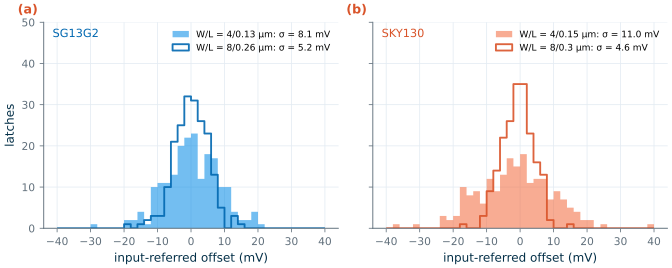
To measure it, we placed 200 latches with the PDKs’ mismatch models in one netlist and found each latch’s trip point by bisection: eleven simulations, each of one decision, with each latch’s input set halfway between the largest input it had decided as 0 and the smallest it had decided as 1, which resolves the trip point to 0.08 mV. A check run confirmed that every simulation draws the same random devices. Figure 20.4 shows the result. For the input pair of Figure 20.1 the offset has σ = 8.1 mV in SG13G2 and 11.0 mV in SKY130. Eq. (20.5) gives 7.9 and 7.2 mV for the pair alone: in SG13G2 the pair accounts for almost all of the offset, in SKY130 the rest of the latch adds about 8 mV in quadrature. With four times the pair area (8 µm by 2Lmin), σ falls to 5.2 and 4.6 mV, against 3.9 and 3.6 mV predicted for the pair: the share of the rest of the latch, 3.4 and 2.9 mV, grows, and further increases of the pair’s area pay off less. The mean offsets, 0.4 and −1.4 mV, are within twice the statistical uncertainty of 200 samples (0.6 and 0.8 mV).
20.7 Noise
Close to its offset, a comparator’s decision becomes random, because the noise of its transistors adds to the input during the integration phase. During integration the input pair’s drain currents charge the capacitances of P and Q, so the difference they integrate is \(g_m\Delta V_{in}\) per unit capacitance and time, and the channel noise of the two transistors integrates the same way. If \(g_m\) changes during the integration, the input-referred noise is approximately [106]
\[\sigma_n^2 \approx \frac{4kT\gamma}{\int g_m\,dt}, \tag{20.6}\]where the integral runs over the integration phase. A longer integration, or a larger \(g_m\), averages the noise over more time. The usual way to measure the noise is the probability of a 1 against the input, which follows a cumulative Gaussian distribution of width \(\sigma_n\). ngspice cannot simulate the noise of transistors in a transient simulation (its transient noise sources are independent sources only), so this chapter does not quote a simulated value; noise matters because, unlike offset, it cannot be calibrated away: in a converter whose comparator offset is corrected, the noise of Eq. (20.6) is what limits the comparator.
20.8 Kickback
The nodes P and Q swing from \(V_{DD}\) to ground in every decision, and the gate-drain capacitances of \(M_1\) and \(M_2\) couple these steps back to the inputs. The circuit that drives the comparator, a resistor ladder in a flash converter, a capacitor array in a successive-approximation converter, sees a disturbance at every clock edge: kickback [105]. Its common-mode part does no harm if both inputs see the same impedance; its differential part, which appears once the latch has decided, corrupts the input of the next decision unless it has died away.
Figure 20.5 shows the disturbance at the inputs of the latch of Figure 20.1 when they are driven through 10 kΩ, a high-impedance source. At the rising clock edge the inputs dip by 248 mV in SG13G2 and 222 mV in SKY130, common mode, as the tail node falls; at the reset edge they jump by 452 and 296 mV, as P and Q are recharged. The differential disturbance, 37 and 29 mV during the decision and 59 and 54 mV at reset, is far larger than the 1 mV input, but it decays within 0.4 ns through the 10 kΩ. A lower source impedance, a preamplifier in front of the latch, or isolation switches that disconnect the inputs during regeneration reduce it.
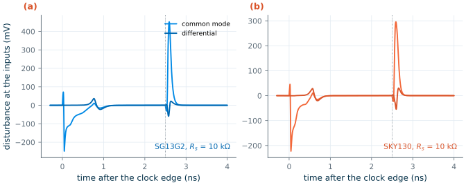
Table 20.1. The StrongARM latch of Figure 20.1 in both PDKs (simulated, tt, 27 °C).
| SG13G2 | SKY130 | |
|---|---|---|
| Regeneration time constant τ | 60.7 ps | 47.9 ps |
| Delay, 1 mV input | 512 ps | 413 ps |
| Extra delay per decade of smaller input | 139 ps | 110 ps |
| Energy per decision | 77 fJ | 145 fJ |
| Unresolved input after 0.5 ns | 1.2 mV | 0.16 mV |
| Offset σ, input pair 4/Lmin | 8.1 mV | 11.0 mV |
| Offset σ, input pair 8/2Lmin | 5.2 mV | 4.6 mV |
| Kickback, differential, Rs = 10 kΩ | 37 mV | 29 mV |
Try it · The comparator script
Every number in this chapter comes from
tools/figs/ch21_comparators.py:python3 tools/figs/ch21_comparators.py wave delay. Try three changes. (1) Double the load capacitors (CL): by Eq. (20.2), the slope of Figure 20.3a should grow, by how much? (2) Lower the input common mode to \(V_{DD}/3\) insa_delay: the input pair gets less overdrive; what happens to the delay and to the energy? (3) Runmcwith the input pair at W = 16 µm and \(L\) = \(4L_{min}\): does the offset follow Eq. (20.5)?
- An open-loop amplifier resolves a small input in a time proportional to 1/input; a latch, by positive feedback, in a time proportional to ln(1/input), with the regeneration time constant τ = C/gm.
- The StrongARM latch resets, integrates the input on the drains of its input pair, and regenerates; it draws no static current.
- With the same widths, τ is 61 ps in SG13G2 and 48 ps in SKY130: a 1 mV decision takes 0.51 and 0.41 ns, and every decade less input adds 139 and 110 ps. A decision costs 77 and 145 fJ.
- Metastability follows from τ: with 0.5 ns to decide, inputs below 1.2 mV (SG13G2) and 0.16 mV (SKY130) are not resolved, and every extra τ divides the threshold by e.
- The offset is several millivolts: σ = 8.1 mV (SG13G2) and 11.0 mV (SKY130) for a 4 µm/Lmin input pair, close to AVT/√(WL) in SG13G2; four times the area gives 5.2 and 4.6 mV. A converter with a smaller LSB needs offset calibration or a preamplifier with offset cancellation.
- Kickback through the input pair’s gate-drain capacitance disturbs a 10 kΩ source by hundreds of millivolts common mode and tens of millivolts differentially; drive comparators from low impedances or isolate them.
Further reading
- B. Razavi, “The StrongARM latch” [107]: a compact analysis of the three phases, delay and noise; and B. Razavi and B. A. Wooley [102] on preamplifiers and offset cancellation for high-resolution comparators.
- T. Kobayashi et al. [103]: the current-controlled latch sense amplifier that became the StrongARM latch.
- B. Wicht, T. Nirschl and D. Schmitt-Landsiedel [104]: how each transistor of a latch contributes to its offset, and how to size it for yield and speed.
- P. Nuzzo et al. [106]: the noise of regenerative comparators, phase by phase.
- H. J. M. Veendrick [101] on metastability and its failure rate; P. M. Figueiredo and J. C. Vital [105] on kickback and how to reduce it.